S6A0065 Просмотр технического описания (PDF) - Samsung
Номер в каталоге
Компоненты Описание
производитель
S6A0065 Datasheet PDF : 12 Pages
| |||
S6A0065
40 CH SEGMENT/COMMON DRIVER FOR DOT MATRIX LCD
PIN DESCRIPTION
Pin (No.)
VDD(24)
GND(34)
VEE(31)
V1, V2
(44,45)
SC1 - SC20
V3, V4
(46, 47)
SHL1(41)
DL1, DR1
(35, 36)
SC21- SC40
V5, V6
(48, 49)
SHL2(42)
DL2,DR2
(37, 38)
M (40)
CL1,CL2
(32,33)
I/O
Name
Operating Voltage
Power
Negative Supply Voltage
I
Bias Voltage
Description
For logical circuit (2.7 - 5.5V)
0V (GND)
For LCD driver circuit
Bias voltage level for LCD drive (select level)
Interface
Power
Supply
Power
O
LCD driver
LCD driver output
LCD
I
Part 1 Bias Voltage Bias voltage level for LCD drive (non-select level)
Power
I
Data interface Selection of the shift direction of Part 1 shift
VDD or VSS
register
SHL1
VDD
VSS
DL1
out
in
DR1
in
out
I/O
Data input/output of Part 1 shift register
Controller or
S6A0065
O
LCD driver
LCD driver output
I
Part 2 Bias Voltage Bias voltage level for LCD drive (non-select level)
Power
I
Data interface Selection of the shift direction of Part 2 shift
register
SHL2
VDD
VSS
DL2
out
in
DR2
in
out
I/O
Data input/output of Part 2 shift register
I
Alternated signal for LCD
driver output
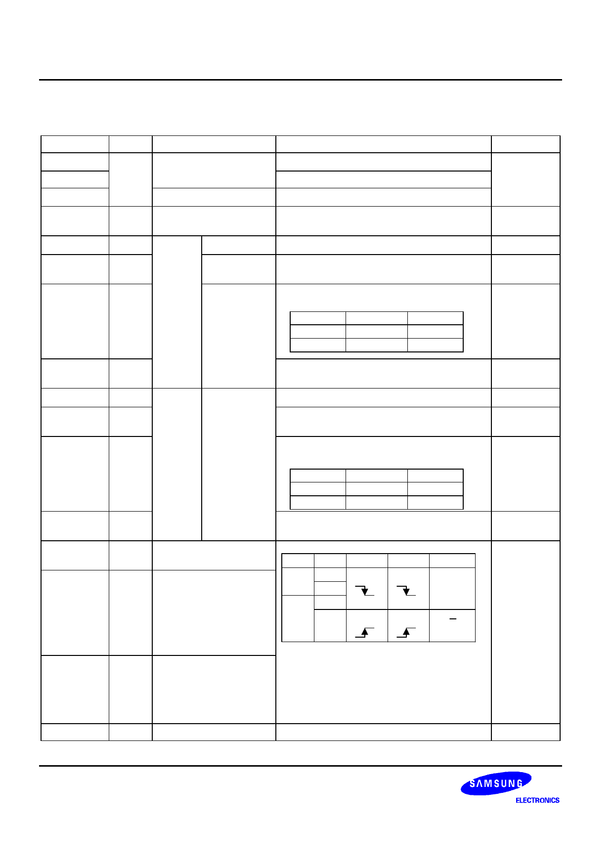
PART FCS
CL1
CL2 M polartty
I
Data shift /latch clock
VSS latch clock shift clock
1
VDD
M
VSS
2
latch clock shift clock
VDD
M
VDD or VSS
Controller or
S6A0065
Controller
FCS(43)
I
Mode selection
NC(39)
Shift/latch clock of display data and polarity of M
signal are changed by FCS signal.
By setting FCS to VDD level, user can select the
function that use Part 1 as segment driver and
Part 2 as common driver simultaneously.
No connection pin
NC
6
Share Link: 