S5K433CA Просмотр технического описания (PDF) - Samsung
Номер в каталоге
Компоненты Описание
производитель
S5K433CA Datasheet PDF : 25 Pages
| |||
S5K433CA, S5K433LA
1/4” VGA CMOS IMAGE SENSOR
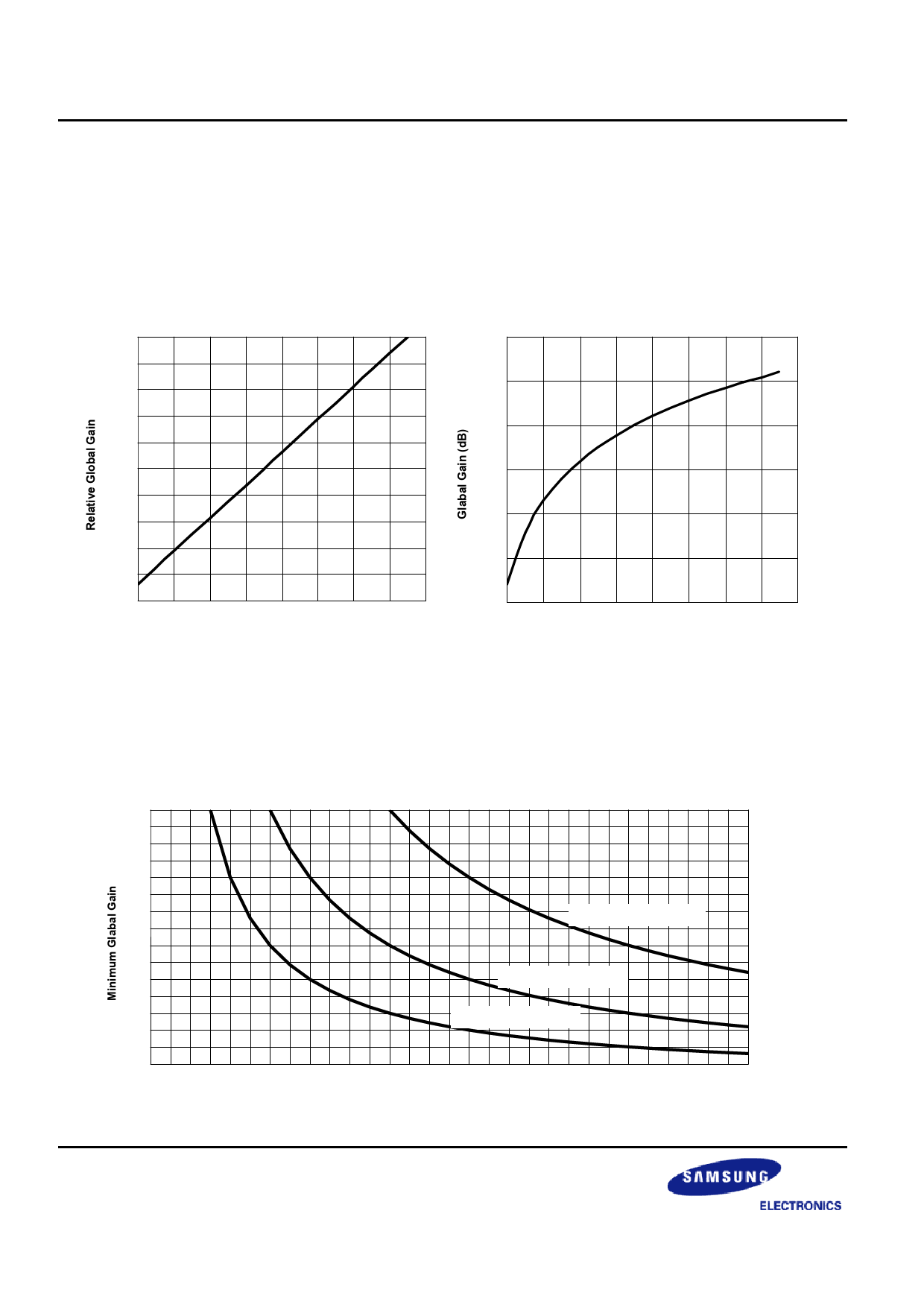
2-4. Quadrisectional Global Gain Control
The user can controls the global gain to change the gain for all color channels by the Global Gain Control
Registers (sgg1, sgg2, sgg3, sgg4). The global gain control register is composed of four register groups and
each register value decides the gain for each quarter section of output code level.
Global Gain = (sgg[3:0]+1) / 8
2.0
1.8
1.6
1.4
1.2
1.0
0.8
0.6
0.4
0.2
0.0
0
2
4
6
8 10 12 14 16
Program m able Gain Control
10
5
0
-5
-10
-15
-20
0
2
4
6
8 10 12 14 16
Program m able Gain Control
Figure 7. Relative Global Gain
The ADC gain is dependent on MCLK frequency (not on DCLK frequency) and ADC resolution. The default
global gain is set for typical MCLK frequency (24MHz) and 10-bit ADC. When the frequency and ADC resolution is
changed, the average global gain, (sgg1+sgg2+sgg3+sgg4+4)/32 should be changed to maintain the resulting
gain over unity for assuring appropriate ADC conversion range.
15
14
13
12
11
10
9
10-bit ADC resolution
8
7
6
5
9-bit ADC resolution
4
3
8-bit ADC resolution
2
1
0
0 1 2 3 4 5 6 7 8 9 10 11 12 13 14 15 16 17 18 19 20 21 22 23 24 25 26 27 28 29 30
MCLK frequency (MHz)
Figure 8. Recommended Minimum Global Gain Control Value
20
Share Link: 