S5K433CA Просмотр технического описания (PDF) - Samsung
Номер в каталоге
Компоненты Описание
производитель
S5K433CA Datasheet PDF : 25 Pages
| |||
S5K433CA, S5K433LA
1/4” VGA CMOS IMAGE SENSOR
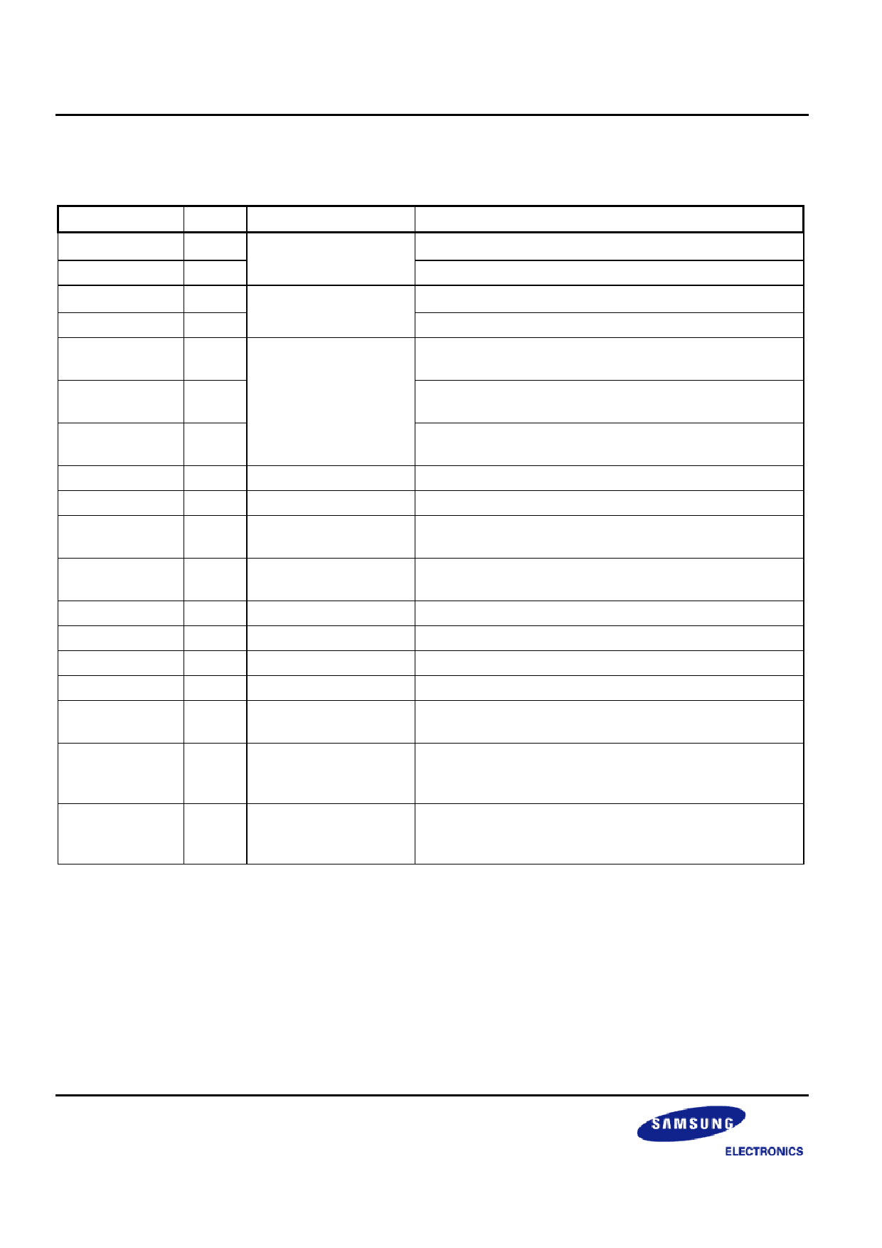
PIN DESCRIPTION
Pin No
VDDD (24)
VSSD (1)
VDDIO (26, 35)
VSSIO (47, 38)
VDDA
(4, 21, 34, 39)
VSSA
(3, 22, 33, 40)
VBBA
(2, 23, 32, 41)
MCLK (46)
RSTN (43)
STBYN (42)
I/O
Power
Power
Power
Power
Power
Name
Digital power supply
I/O power supply
Analog power supply
Power
Power
I Master clock
I Reset
I Standby
DATA0~DATA9
(6, 9~16, 19)
DCLK (27)
HSYNC (28)
VSYNC (29)
SCL (45)
SDA (44)
O Image data output
O Data clock
O Horizontal sync clock
O Vertical sync clock
I Serial interface clock
I/O Serial interface data
TEST1 (30)
I Test input 1
TEST2 (31)
I Test input 2
Function
For logical circuit ( VDD ± 10% )
0V (GND)
For I/O circuit ( VDD ± 10% )
0V (GND)
For analog circuit ( VDD ± 10% )
0V (GND)
For analog circuit bulk bias ( 0V)
Master clock pulse input for all timing generators.
Initializing all the device registers. (Active low)
Activating power saving mode.
( high=normal operation, low=power saving mode )
10-bit image data outputs. When ADC resolution is
reduced, the unused lower bits are set to 0.
Image data output synchronizing pulse output.
Horizontal synchronizing pulse or data valid signal output.
Vertical synchronizing pulse or line valid signal output.
I2C serial interface clock input
I2C serial interface data bus
(external pull-up resistor required)
Test input signal. Though it can be opened in normal
operation (internally pulled down), it is recommended to
ground the test pins.
Test input signal. Though it can be opened in normal
operation (internally pulled down), it is recommended to
ground the test pins.
12
Share Link: 