S3C7238 Просмотр технического описания (PDF) - Samsung
Номер в каталоге
Компоненты Описание
производитель
S3C7238 Datasheet PDF : 36 Pages
| |||
PRODUCT OVERVIEW
S3C7238/P7238/C7235/P7235
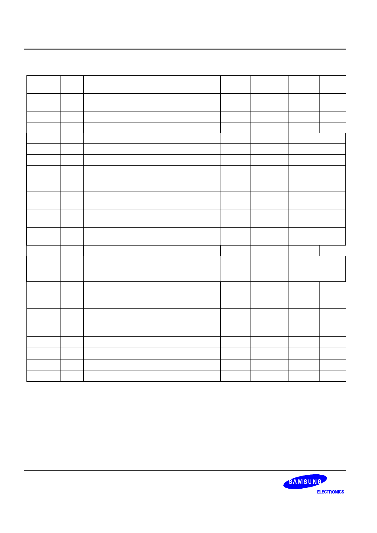
Table 1-1. S3C7238/C7235 Pin Descriptions (Continued)
Pin Name Pin
Type
Description
LCDSY
I/O LCD synchronization clock output for LCD
display expansion
TCL0
I/O External clock input for timer/counter 0
TCLO0
I/O Timer/counter 0 clock output
SI
I Serial interface data input
SO
I/O Serial interface data output
SCK
I/O Serial I/O interface clock signal
INT0
INT1
I External interrupts. The triggering edge for
INT0 and INT1 is selectable. Only INT0 is
synchronized with the system clock.
INT2
I Quasi-interrupt with detection of rising edge
signals.
INT4
I External interrupt input with detection of rising
or falling edge
KS0–KS7 I/O Quasi-interrupt inputs with falling edge
detection.
CLO
I/O CPU clock output
BUZ
I/O 2, 4, 8 or 16 kHz frequency output for buzzer
sound with 4.19 MHz main system clock or
32.768 kHz subsystem clock.
XIN,
XOUT
– Crystal, ceramic or RC oscillator pins for main
system clock. (For external clock input, use
XIN and input XIN‘s reverse phase to XOUT)
XTIN,
XTOUT
– Crystal oscillator pins for subsystem clock.
(For external clock input, use XTIN and input
XTIN's reverse phase to XTOUT)
VDD
– Main power supply
VSS
– Ground
RESET
– Reset signal
TEST
– Test signal input (must be connected to VSS)
Number
33
27
28
23
22
21
24
25
26
20
44–51
30
31
15,14
17,18
12
13
19
16
Share
Pin
P3.1
P1.3
P2.0
P0.3
P0.2
P0.1
P1.0
P1.1
P1.2
P0.0
P6.0–P7.3
P2.2
P2.3
–
–
–
–
–
–
NOTES:
1. Pull-up resistors for all I/O ports are automatically disabled if they are configured to output mode.
2. D * Type has a schmitt trigger circuit at input.
Reset
Value
Input
Input
Input
Input
Input
Input
Input
Input
Input
Input
Input
Input
–
–
–
–
Input
–
Circuit
Type
D
A-1
D
A-1
D*
D*
A-1
A-1
A-1
D*
D
D
–
–
–
–
B
–
1-6
Share Link: 