S-8243BAFFT-TB-G(Rev2_4) Просмотр технического описания (PDF) - Seiko Instruments Inc
Номер в каталоге
Компоненты Описание
производитель
S-8243BAFFT-TB-G
(Rev.:Rev2_4)
(Rev.:Rev2_4)
Seiko Instruments Inc

S-8243BAFFT-TB-G Datasheet PDF : 34 Pages
| |||
BATTERY PROTECTION IC FOR 3-SERIAL OR 4-SERIAL CELL PACK
S-8243A/B Series
Rev.2.4_00
(2) S-8243B Series
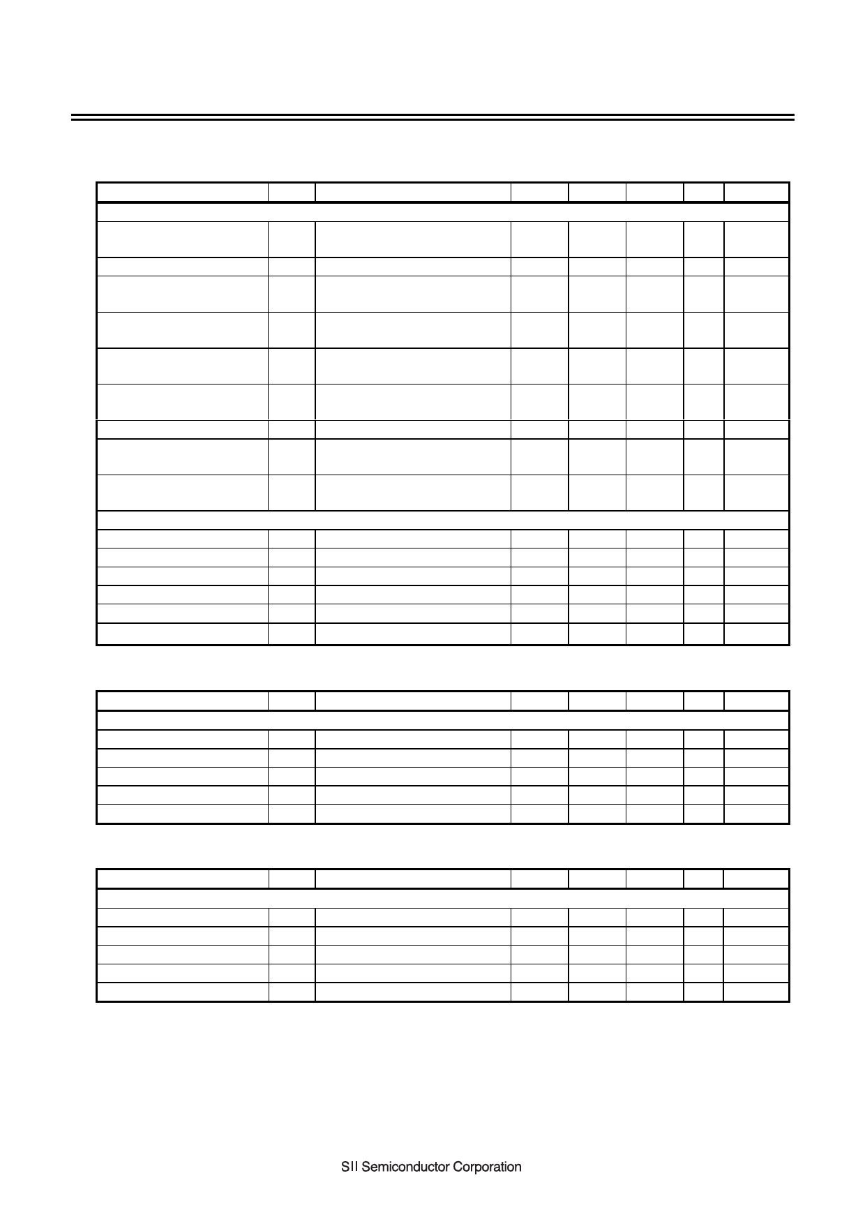
Table 7 (1/2)
(Ta = 25°C unless otherwise specified)
Item
Symbol
Conditions
Min.
Typ.
Max. Unit Test circuit
DETECTION VOLTAGE
Overcharge detection voltage n
n=1, 2, 3, 4
VCUn 3.9 V to 4.4 V, 50 mV Step
VCUn
−0.025
VCun
VCUn
V
+0.025
4
Hysteresis voltage n of overcharge
detection
VHCn −0.10 V to −0.40 V, and 0 V
VHCn
−0.05
VHCn
VHCn
V
+0.05
4
n=1, 2, 3, 4
Overdischarge detection voltage
n=1, 2, 3, 4
VDLn 2.0 V to 3.0 V, 100 mV Step
VDLn
−0.08
VDLn
VDLn
V
+0.08
4
Hysteresis voltage n of
overdischarge detection
n=1, 2, 3, 4
VHDn
0.20 to 0.70, and 0
VHDn
−0.10
VHDn
VHDn
V
+0.10
4
Overcurrent detection voltage 1
VIOV1
0.05 V to 0.3 V, 50 mV Step
VIOV1
−0.025
VIOV1
VIOV1
V
+0.025
4
Overcurrent detection voltage 2
VIOV2
⎯
VDD−0.60 VDD−0.50 VDD−0.40 V
4
Overcurrent detection voltage 3
VIOV3
⎯
VDD
VDD
VDD
V
4
×0.425
×0.5
×0.575
Temperature coefficient for
detection and release voltage*1
TCOE1
Ta= −5°C to +55°C
−1.0
0
1.0 mV/°C
4
Temperature coefficient for
overcurrent detection voltage*2
TCOE2
Ta= −5°C to +55°C
−0.5
0
0.5 mV/°C
4
0 V BATTERY CHARGING FUNCTION (The 0 V battery function is either "0 V battery charging is allowed." or "0 V battery charging is
inhibited." depending upon the product type.)
0 V battery charge starting charger
voltage
V0CHA 0 V battery charging allowed
⎯
0.8
1.5
V
7
0 V battery charge inhibition battery
voltage
V0INH 0 V battery charging inhibited
0.4
0.7
1.1
V
7
INTERNAL RESISTANCE
Internal resistance between VMP
and VDD
RVDM
V1=V2=V3=V4=3.5 V
500
1100
2400
kΩ
8
Internal resistance between VMP
and VSS
RVSM
V1=V2=V3=V4=1.8 V
300
700
1500
kΩ
8
VOLTAGE REGULATOR
Output voltage
Line regulation
Load regulation
BATTERY MONITOR AMP
VOUT
VDD=14V, IOUT=3 mA
3.221
3.300
3.379
V
2
ΔVOUT1 VDD=6 V→18 V, IOUT=3 mA
⎯
5
15
mV
2
ΔVOUT2 VDD=14 V, IOUT=5 μA→3 mA
⎯
15
30
mV
2
Input offset voltage n
n=1, 2, 3, 4
VOFFn
V1=V2=V3= V4=3.5 V
60
165
270
mV
3
Voltage gain n
n=1, 2, 3, 4
GAMPn V1=V2=V3= V4=3.5 V
0.2×0.99
0.2
0.2×1.01 ⎯
3
INPUT VOLTAGE, OPERATING VOLTAGE
Operating voltage between VDD
and VSS
VDSOP
⎯
6
⎯
18
V
4
CTL1 input voltage for High
VCTL1H
⎯
VDD×0.8
⎯
⎯
V
6
CTL1 input voltage for Low
VCTL1L
⎯
⎯
⎯
VDD×0.2
V
6
CTLn input voltage for High
n=2, 3, 4
VCTLnH
⎯
VOUT×0.9
⎯
VOUT
V
3, 6
CTLn input voltage for Low
n=2, 3, 4
VCTLnL
⎯
⎯
⎯
VOUT×0.1
V
3, 6
10
Seiko Instruments Inc.
Share Link: