RT9702 Просмотр технического описания (PDF) - Richtek Technology
Номер в каталоге
Компоненты Описание
производитель
RT9702 Datasheet PDF : 16 Pages
| |||
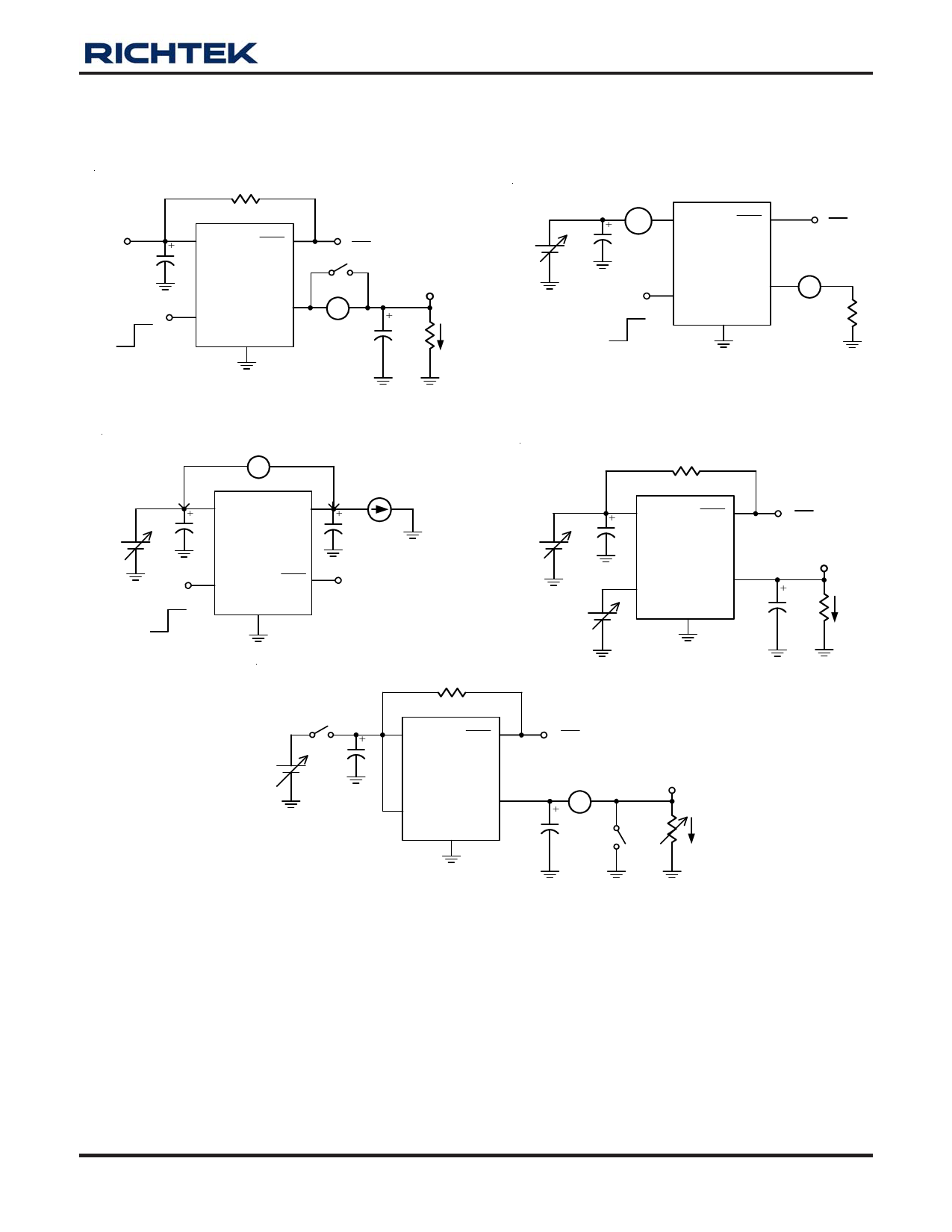
Test Circuits
1
RFG
VIN
CIN
Chip Enable
VIN
FLG
RT9702/A
VOUT
EN
GND
VFLG
S1
IOUT
A
COUT
VOUT
RL IL
RT9702/A
2
ISupply
A
VIN
FLG
VFLG
VIN
CIN
RT9702/A
ILEAK AGE
Chip Enable
VOUT
EN
GND
A
RL
3
VRDS(ON)
V
CIN
VIN
Chip Enable
VIN VOUT
RT9702/A
EN
FLG
GND
IOUT
COUT
4
VIN
CIN
VCE
RFG
VIN
FLG
VFLG
RT9702/A
VOUT
EN
GND
COUT
VOUT
RL IL
5
S2
VIN
CIN
RFG
VIN
FLG
RT9702/A
VOUT
EN
GND
VFLG
COUT
IOUT
A
VOUT
S3 RL
IL
Note: Above test circuits reflected the graphs shown on “ Typical Operating Characteristics ” are as follows:
1−Turn-On Rising & Falling Time vs. Temperature, Turn-On & Off Response, Flag Response
2−Supply Current vs. Input Voltage & Temperature, Switch Off Supply Current vs. Temperature, Turn-Off Leakage Current
vs. Temperature
3−On-Resistance vs. Input Voltage & Temperature
4−EN Threshold Voltage vs. Input Voltage & Temperature, Flag Delay Time vs. Input Voltage & Temperature, UVLO
Threshold vs. Temperature, UVLO at Rising & Falling
5−Current Limit vs. Input Voltage/Temperature, Short Circuit Current Response, Short Circuit Current vs. Temperature,
Inrush Current Response, Soft-start Response, Ramped Load Response, Current Limit Transient Response, Thermal
Shutdown Response
DS9702/A-11 June 2007
www.richtek.com
3
Share Link: 