RT8113 Просмотр технического описания (PDF) - Richtek Technology
Номер в каталоге
Компоненты Описание
производитель
RT8113 Datasheet PDF : 21 Pages
| |||
RT8113
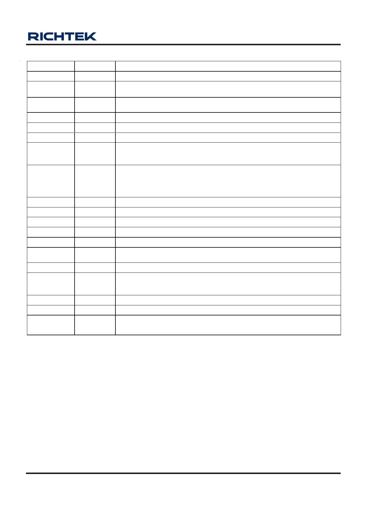
Functional Pin Description
Pin No.
Pin Name
Pin Function
2
OCSET
Over Current Protection Threshold Set Pin.
3
FBRTN
Return Ground. This pin is Negative Node of the differential Remote Voltage
sending.
4
SS
Soft-Start Ramp Slope Set Pin. Connect this pin to FBRTN by a Capacitor to
Adjust soft-start slew rate.
5
COMP
Compensation Pin. Output of Error Amplifier and Input of PWM comparator.
6
FB
Inverting Input of Error Amplifier.
7
ADJ
Droop Set Pin. Connect a resistor from this pin to GND sets the load line slope.
8
OFS
Voltage Offset Pin. This pin sets No-Load Output Voltage Offset. Connect a
resistor from this Pin to VCC5 or GND to bidirection set the output voltage
no-load offset.
Switching Frequency Set Pin. Connect this pin to GND via a resistor to adjust
9
RT/EN
switching frequency and operate with droop function.
Connect this pin to VCC5 via a resistor to adjust switching frequency and operate
without droop function.
10
VCC5
Internal 5V Regulator Output.
11
ISP
Non-Invertering Input of Current Sense Amplifier.
12
ISN
Invertering Input of Current Sense Amplifier.
13
LGATE
Lower Gate Driver. This pin drives the gate of low side MOSFETs.
14
VCC12
12V Power Supply Input Pin.
15
PHASE
Switch Node of High side Driver. Connect this pin to high-side MOSFETs sources
together with the low side MOSFETs drains and inductor.
16
UGATE
Upper Gate Driver. This pin drives the gate of the high-side MOSFETs.
Bootstrap Power Pin. This pin powers the high-side MOSFETs drivers. Connect
17
BOOT
this pin to the junction of the bootstrap capacitor with the cathode of the bootstrap
diode.
18
PGOOD
Power Good Indicator.
19 to 24,1 VID7 to VID1 DAC Voltage Identification Inputs.
25
(Exposed Pad)
GND
Ground Pin. The exposed pad must be soldered to a large PCB and connected to
AGND for maximum power dissipation.
DS8113-02 April 2011
www.richtek.com
3
Share Link: 