RT8011 Просмотр технического описания (PDF) - Richtek Technology
Номер в каталоге
Компоненты Описание
производитель
RT8011 Datasheet PDF : 17 Pages
| |||
RT8011/A
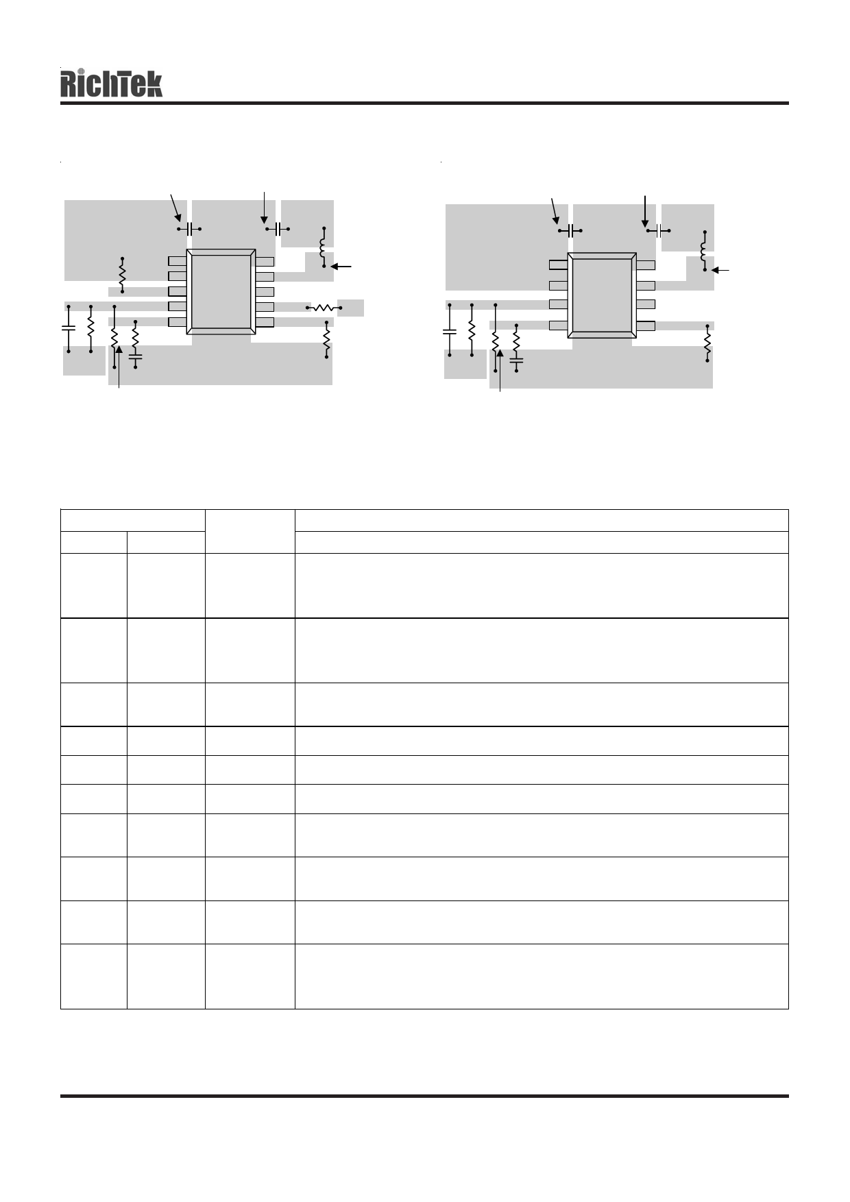
Layout Guide
CIN must be placed between
VDD and GND as closer as
possible
VIN
CIN
GND
PVDD
RT8011
6
5
Output capacitor must
be near RT8011
COUT VOUT
L1
PGND
LX should be
connected to
Inductor by wide
and short trace,
keep sensitive
compontents away
from this trace
VDD
7
4
LX
PGOOD
8
3
GND
FB
9
COMP
10
R1
CF
R2 RCOMP
2
SYNC
VIN
1
SHDN/RT
ROSC
VOUT
CCOMP
GND
Connect the FB pin directly to feedback resistors. The
resistor divider must be connected between VOUT and
GND.
Figure 3. RT8011 Layout Guide
CIN must be placed between
VDD and GND as closer as
possible
VIN
CIN
GND
PVDD
RT8011A
5
4
Output capacitor must
be near RT8011A
COUT VOUT
L1
PGND
LX should be
connected to
Inductor by wide
and short trace,
keep sensitive
compontents away
from this trace
VDD
6
FB
7
3
LX
2
GND
COMP
8
R1
CF
R2 RCOMP
1
SHDN/RT
ROSC
VOUT
CCOMP
GND
Connect the FB pin directly to feedback resistors. The
resistor divider must be connected between VOUT and
GND.
Figure 4. RT8011A Layout Guide
Functional Pin Description
Pin Number
Pin Name
RT8011 RT8011A
1
1
SHDN/RT
2
-- SYNC
3
2
GND
Pin Function
Oscillator Resistor Input. Connecting a resistor to ground from this pin sets
the switching frequency. Forcing this pin to VDD causes the device to be shut
down.
External Clock Synchronization Input. The oscillation frequency can be
synchronized to an external oscillation applied to this pin. When tied to VDD,
internal oscillator is selected.
Signal Ground. All small-signal components and compensation components
should connect to this ground, which in turn connects to PGND at one point.
4
3
LX
Internal Power MOSFET Switches Output. Connect this pin to the inductor.
5
4
PGND
Power Ground. Connect this pin close to the (−) terminal of CIN and COUT.
6
5
PVDD
Power Input Supply. Decouple this pin to PGND with a capacitor.
7
6
VDD
Signal Input Supply. Decouple this pin to GND with a capacitor. Normally VDD
is equal to PVDD.
Power Good Indicator. Open-drain logic output that is pulled to ground when
8
--
PGOOD
the output voltage is not within ±12.5% of regulation point.
9
7
FB
Feedback Pin. Receives the feedback voltage from a resistive divider
connected across the output.
Error Amplifier Compensation Point. The current comparator threshold
10
8
COMP
increases with this control voltage. Connect external compensation elements
to this pin to stabilize the control loop.
DS8011/A-00 August 2006
www.richtek.com
3
Share Link: 