RF3159 Просмотр технического описания (PDF) - RF Micro Devices
Номер в каталоге
Компоненты Описание
производитель
RF3159 Datasheet PDF : 26 Pages
| |||
RF3159
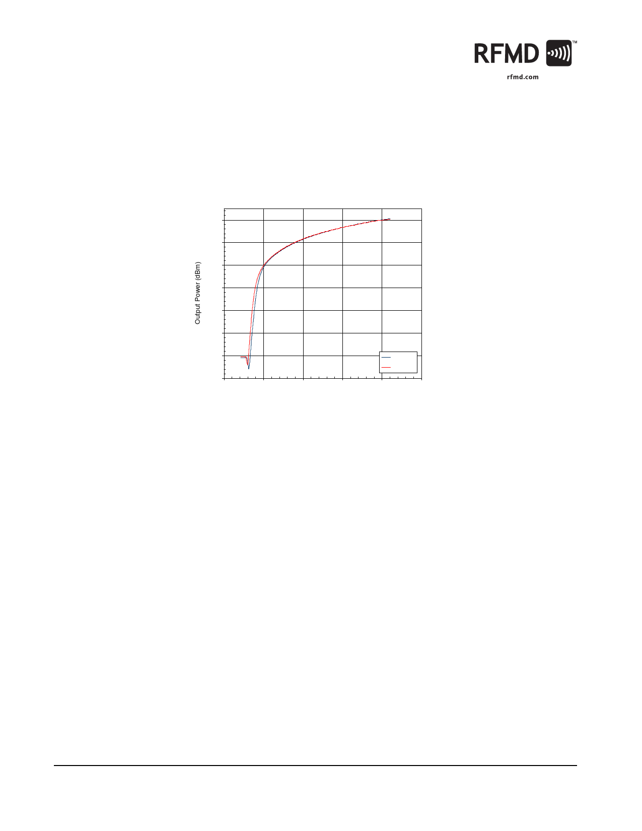
The VRAMP voltage range should be limited to min and max values in the specifications to avoid damage or undesirable opera-
tion. At some voltage below 0.35V, the CMOS controller switches off and turns off the PA. The effect of this is a discontinuity in
the response curve. In order to guarantee minimum switching transients, it is recommended that the minimum ramp voltage
be set slightly above the voltage where this discontinuity occurs (See Figure 3). The VRAMP voltage at which the discontinuity
occurs is unique to the design of the part and does not shift significantly across process. Figure 3 shows the power versus
VRAMP response curve for two parts which represent typical process variation of the discontinuity.
Low Band POUT versus VRAMP
824MHz, 3.6V, PIN=2dBm
35.0
25.0
15.0
5.0
-5.0
-15.0
-25.0
-35.0
0.0
0.5
Figure 3. Graph of Output Power versus VRAMP
1.0
1.5
VRAMP (V)
Sample 1
Sample 2
2.0
2.5
As the VRAMP voltage approaches its maximum, the linear regulator in the CMOS saturates, the output power reaches its maxi-
mum level, and the VRAMP versus Output Power curve levels out. The saturation point of the linear regulator is directly propor-
tional to the VBATT supply voltage applied. The VRAMP voltage can be increased above the saturation level, but the PA will not
produce any higher output power. It is not recommended to apply a VRAMP voltage above the absolute maximum specification,
as the part could be damaged.
When the FET pass-device in the linear regulator saturates, the response time of the regulated voltage slows significantly. If the
control voltage changes (as in ramp-down) the saturated linear regulator does not react fast enough to follow the ramp-down
curve. The result is a discontinuity in the output power ramp and degraded switching transients. This usually occurs at low
VBATT levels where the regulated VCC voltage is very near the supply voltage. The RF3159 incorporates a saturation detection
circuit which senses if the FET pass-device is entering saturation and reduces VCC to prevent it. This relieves the requirement of
the transceiver controller to adjust the maximum VRAMP when the battery voltage is low.
Design Considerations
There are several key factors to consider in the implementation of a mobile phone transmitter solution using the RF3159:
• System efficiency:
The RF output match can be designed to improve system efficiency by presenting a non 50Ω load. Output matching circuits for
the RF3159 should be a compromise between system efficiency and power as well as EDGE linearity. Optimal matching for
GSM mode alone may degrade the linear performance beyond system specifications.
20 of 26
7628 Thorndike Road, Greensboro, NC 27409-9421 · For sales or technical
support, contact RFMD at (+1) 336-678-5570 or sales-support@rfmd.com.
Rev A0 DS070102
Share Link: 