RF3133 Просмотр технического описания (PDF) - RF Micro Devices
Номер в каталоге
Компоненты Описание
производитель
RF3133 Datasheet PDF : 16 Pages
| |||
RF3133
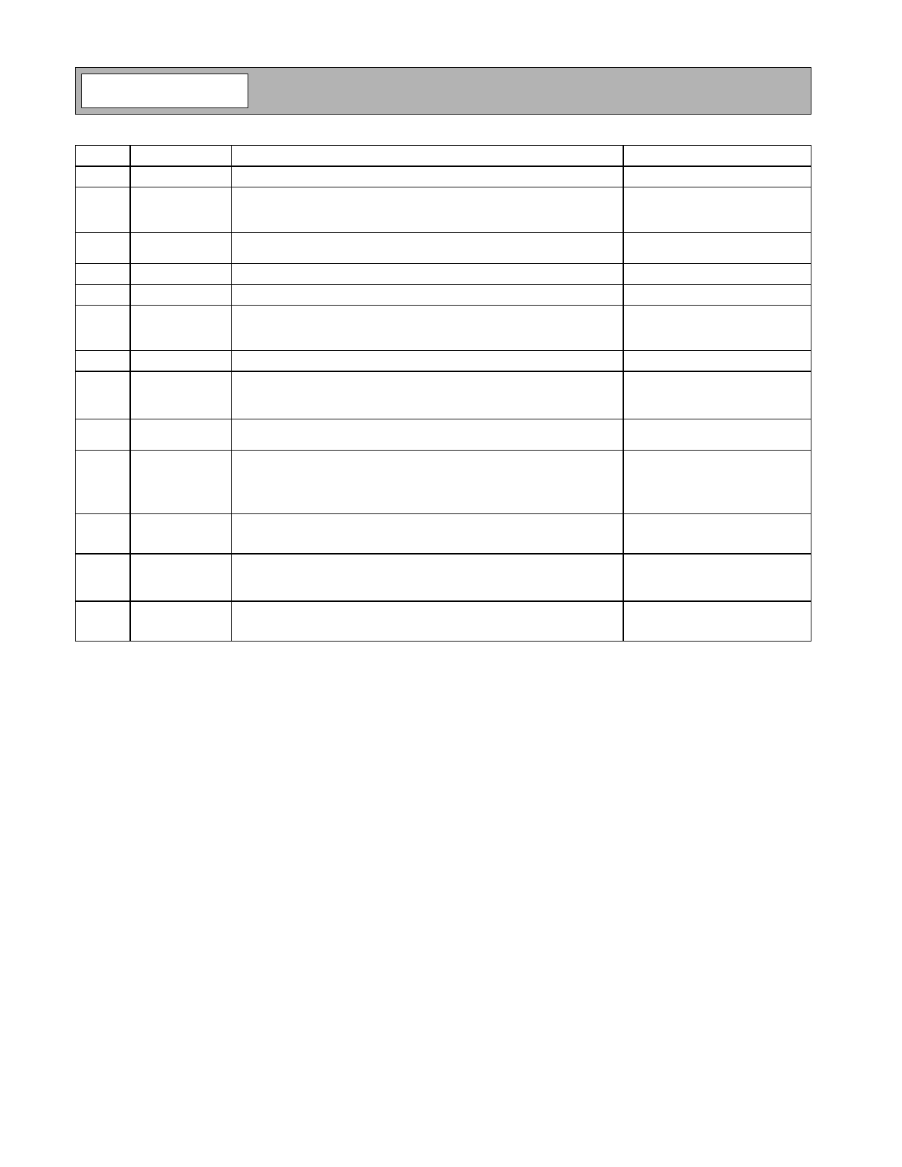
Pin
1
2
3
4
5
6
7
8
9
10
11
12
Pkg
Base
Function Description
DCS/PCS IN RF input to the DCS band. This is a 50Ω input.
BAND
SELECT
Allows external control to select the GSM or DCS band with a logic high
or low. A logic low enables the GSM band whereas a logic high enables
the DCS band.
TX ENABLE This signal enables the PA module for operation with a logic high. Once
TX Enable is asserted the RF output level will increase to -2dBm.
VBATT
Power supply for the module. This should be connected to the battery.
VREG
Regulated voltage input for power control function. (2.8V nom)
VRAMP
Ramping signal from DAC. A simple RC filter may need to be con-
nected between the DAC output and the VRAMP input depending on
the baseband selected.
GSM IN RF input to the GSM band. This is a 50Ω input.
VCC2
Controlled voltage input to driver stage for GSM bands. This voltage is
part of the power control function for the module. This node must be
connected to VCC out.
GSM OUT RF output for the GSM band. This is a 50Ω output. The output load line
matching is contained internal to the package.
VCC OUT
Controlled voltage output to feed VCC2. This voltage is part of the power
control function for the module. It can not be connected to anything
other than VCC2, nor can any component be placed on this node (i.e.,
decoupling capacitor).
DCS/PCS
OUT
RF output for the DCS band. This is a 50Ω output. The output load line
matching is contained internal to the package.
VCC2
Controlled voltage input to DCS driver stage. This voltage is part of the
power control function for the module. This node must be connected to
VCC out.
GND
Interface Schematic
2-464
Rev A6 050909
Share Link: 