RF2948B Просмотр технического описания (PDF) - RF Micro Devices
Номер в каталоге
Компоненты Описание
производитель
RF2948B Datasheet PDF : 18 Pages
| |||
RF2948B
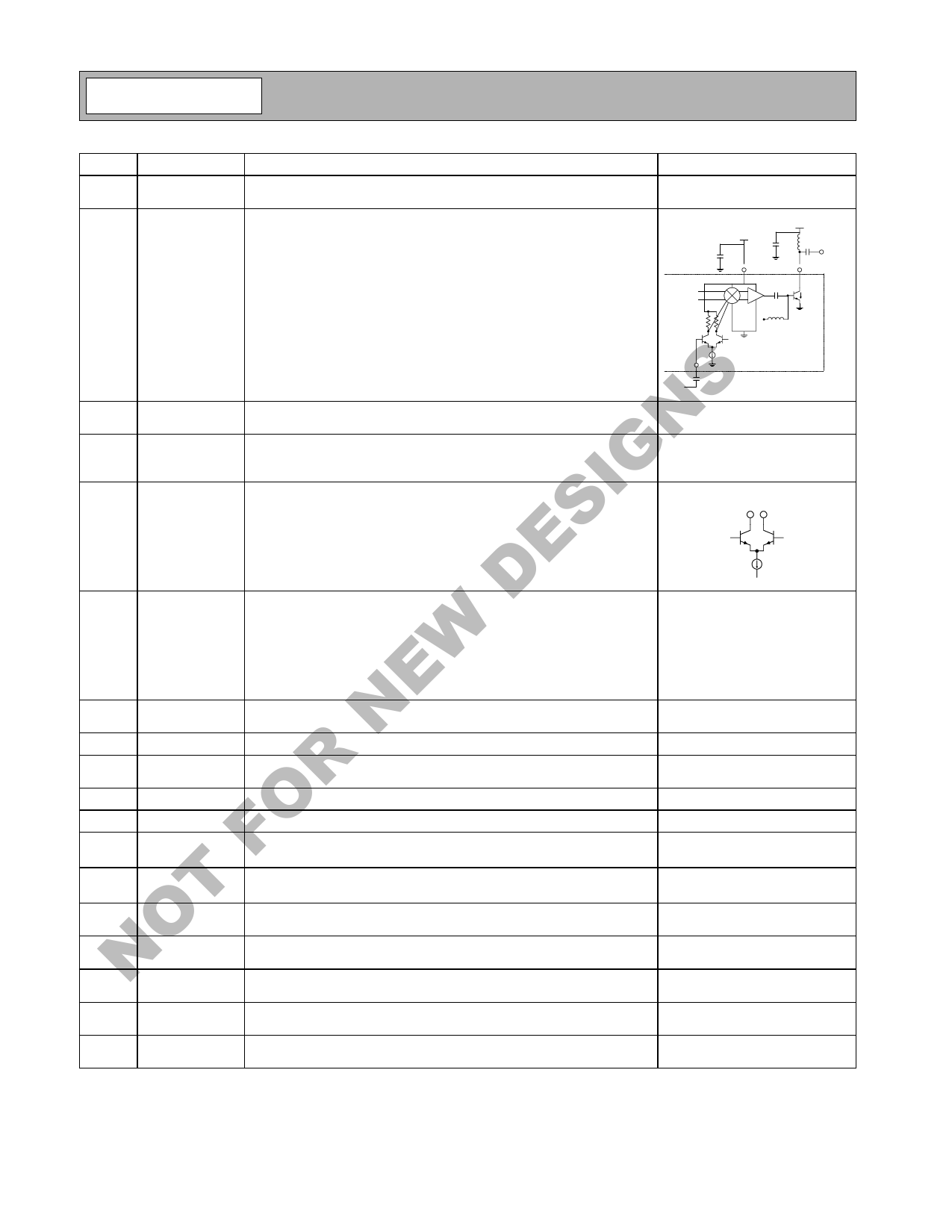
Pin
13
14
Function
PA IN
VCC5
Description
Input to the power amplifier stage. This is a 50Ω input. Requires DC-
blocking/tuning cap.
Supply for the RF LO buffer, RF upconverter and amplifier.
Interface Schematic
See pin 12.
CBYP
22 nF
From
TX VGA
VCC
CBYP
22 nF
VCC5
VB
VCC
To TX RF
Image Filter
RF OUT
12 mA
15
RF LO
16
RF OUT
17 IF1 OUT-
18 IF1 OUT+
19
TXI BP
20 TXI DATA
21
TXQ BP
22 TXQ DATA
23
VCC4
24
I OUT
25
Q OUT
T 26 VREF1 BUF
O 27
DCFB I
N 28 DCFB Q
29 BW CTRL
30
VCC2
RF LO
From
RF VCO
CBLOCK
22 pF
S Single-ended LO input for the transmit upconverter. External matching See pin 14.
to 50Ω and a DC-block are required.
N Upconverted Transmit signal. This 50Ω output is intended to drive an See pin 14.
RF filter to suppress the undesired sideband, harmonics, and other out-
of-band mixer products.
G The inverting open collector output of the quadrature modulator. This
I pin needs to be externally biased and DC isolated from other parts of
the circuit. This output can drive a Balun with IF1 OUT+, to convert to
S unbalanced to drive a SAW filter. The Balun can be either broadband
(transformer) or narrowband (discrete LC matching). Alternatively, just
E IF1 OUT+ can be used to drive a SAW single-ended with an RF choke
(high Z at IF) from VCC to IF1 OUT-.
IF1 OUT+
D The non-inverting open collector output of the quadrature modulator. See pin 17.
This pin needs to be externally biased and DC isolated from other parts
of the circuit. This output can drive a Balun with IF1 OUT-, to convert to
unbalanced to drive a SAW filter. The Balun can be either broadband
(transformer) or narrowband (discrete LC matching). Alternatively, just
W IF1 OUT+ can be used to drive a SAW single-ended with an RF choke
(high Z at IF) from VCC to IF1 OUT+.
E This is the in-phase modulator bypass pin. A 10nF capacitor to ground
N is recommended.
I input to the baseband 5 pole Bessel LPF for the transmit modulator.
This is the quadrature phase modulator bypass pin. A 10nF capacitor
to ground is recommended.
R Q input to the baseband 5 pole Bessel LPF for the transmit modulator.
Power supply for quadrature modulator.
O Baseband analog signal output for in-phase channel.
F700mVP-P linear output.
Baseband analog signal output for quadrature channel.
700mVP-P linear output.
Buffered version of the VREF1 output. See pin 31.
Sink/Source current <1mA.
DC feedback capacitor for in-phase channel. Requires capacitor to
ground. (22nF recommended)
DC feedback capacitor for quadrature channel. Requires decoupling
capacitor to ground. (22nF recommended)
This pin requires a resistor to ground to set the baseband LPF band-
width of the receiver and transmit GmC filter amps.
Supply for the I and Q baseband and GmC filters. This pin should be
bypassed with a 10nF capacitor.
IF1 OUT-
11-244
Rev A6 040930
Share Link: 