REF02CJ Просмотр технического описания (PDF) - Analog Devices
Номер в каталоге
Компоненты Описание
производитель
REF02CJ Datasheet PDF : 16 Pages
| |||
REF02
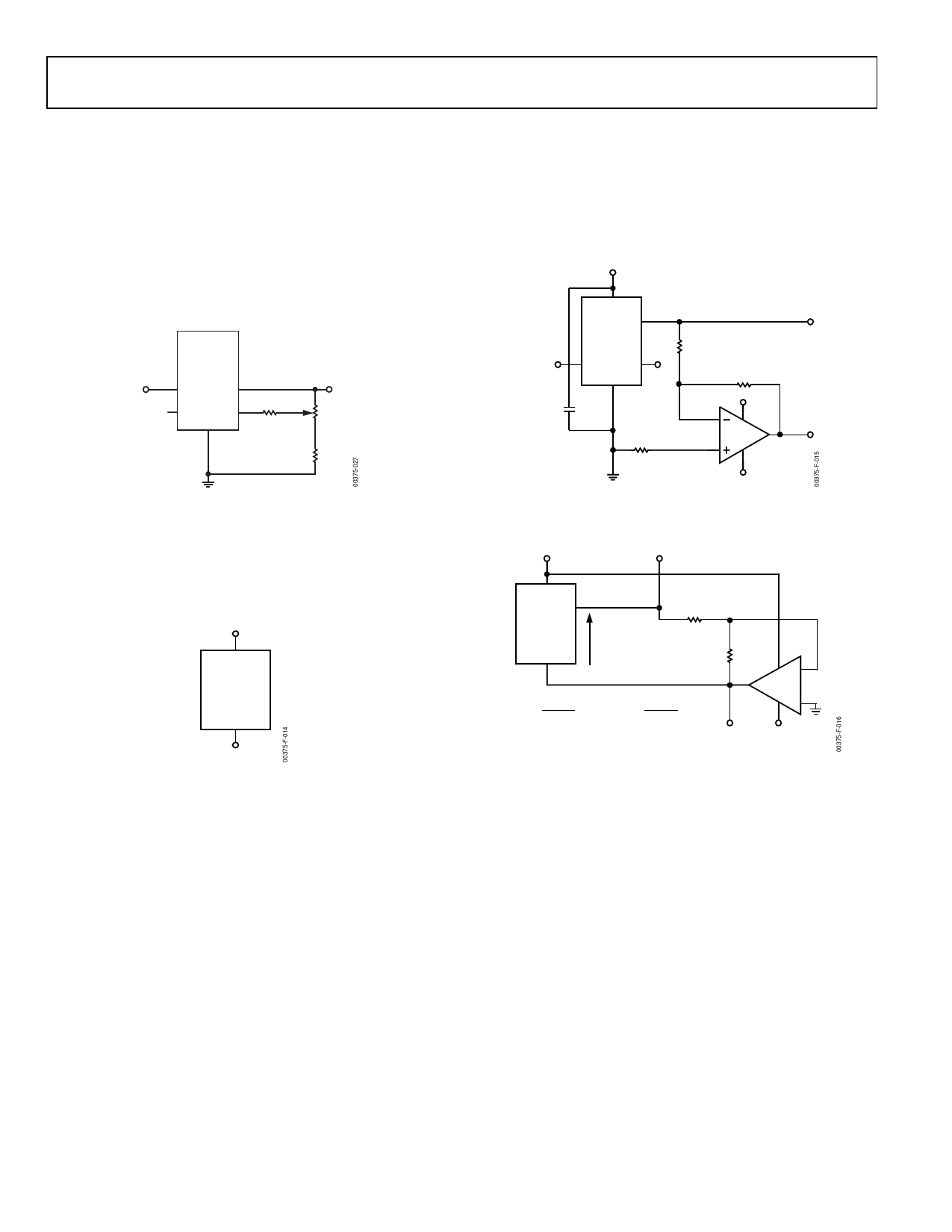
OUTPUT ADJUSTMENT
The REF02 trim terminal can be used to adjust the output
voltage over a 5 V ± 300 mV range. This feature lets the system
designer trim system errors by setting the reference to a voltage
other than 5 V. The output also can be set to exactly 5.00 V or to
5.12 V for binary applications.
U1
REF02
VIN
VIN VOUT
VO
TEMP TRIM
GND
R1
470kΩ
pot
10kΩ
R2
1kΩ
Figure 14. Output Adjustment Circuit
+18V
2
VIN
REF02
GND
4
–18V
Figure 15. Burn-In Circuit
Adjustment of the output does not significantly affect the
temperature performance of the device. The temperature
coefficient change is approximately 0.7 ppm/°C for 100 mV of
output adjustment.
+15V
2
VIN
VO 6
+5V
REF02
3
5
TEMP TRIM
GND
10kΩ
10kΩ
0.1µF
4
5kΩ
+15V
–5V
OP02
–15V
Figure 16. ±5 V Reference
VO+
+5V
+2.5V
2
6
REF02
VREF
4
R1
5.6kΩ
R2
5.6kΩ
6
R1
R2
VO+ = R1 + R2 (VREF), VO– = R1 + R2 (VREF)
+VO
–2.5V
7 –2
OP02
4 +3
–9V
Figure 17. ±2.5 V Reference
Rev. I | Page 10 of 16
Share Link: 