RD74LVC16244B Просмотр технического описания (PDF) - Renesas Electronics
Номер в каталоге
Компоненты Описание
производитель
RD74LVC16244B Datasheet PDF : 9 Pages
| |||
RD74LVC16244B
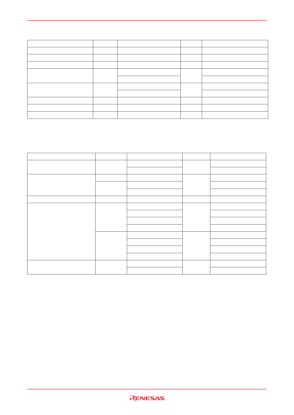
Absolute Maximum Ratings
Item
Symbol
Ratings
Unit
Conditions
Supply voltage
VCC
–0.5 to 7.0
V
Input diode current
IIK
–50
mA VI = –0.5 V
Input voltage
VI
–0.5 to 7.0
V
Output diode current
IOK
–50
mA VO = –0.5 V
50
VO = VCC+0.5 V
Output voltage
VO
–0.5 to VCC +0.5
V Output "H" or "L"
–0.5 to 7.0
Output "Z" or VCC:OFF
Output current
IO
±50
mA
VCC, GND current / pin
ICC or IGND
100
mA
Storage temperature
Tstg
–65 to +150
°C
Note: The absolute maximum ratings are values, which must not individually be exceeded, and furthermore, no two of
which may be realized at the same time.
Recommended Operating Conditions
Item
Symbol
Ratings
Supply voltage
VCC
1.5 to 5.5
1.65 to 5.5
Input / Output voltage
VI
0 to 5.5
VO
0 to VCC
0 to 5.5
Operating temperature
Ta
–40 to 85
Output current
IOH
–4
–8
–12
–24
IOL
4
8
12
Input rise / fall time*1
24
tr, tf
20
10
Notes: 1. This item guarantees maximum limit when one input switches.
Waveform: Refer to test circuit of switching characteristics.
Unit
V
V
°C
mA
mA
ns/V
Conditions
Data hold
At operation
G, A
Output “H” or “L”
Output “Z” or VCC: OFF
VCC = 1.65 V
VCC = 2.3 V
VCC = 2.7 V
VCC = 3.0 V to 5.5 V
VCC = 1.65 V
VCC = 2.3 V
VCC = 2.7 V
VCC = 3.0 V to 5.5 V
VCC = 1.65 V to 2.7 V
VCC = 3.0 V to 5.5 V
Rev.1.00 Mar. 14, 2005 page 3 of 8
Share Link: 