PSD813F1-A Просмотр технического описания (PDF) - STMicroelectronics
Номер в каталоге
Компоненты Описание
производитель
PSD813F1-A Datasheet PDF : 120 Pages
| |||
Preliminary
PSD813F1
Architectural
Overview
(cont.)
PSD813F1-A
5.4 I/O Ports
The PSD813F1 has 27 I/O pins divided among four ports (Port A, B, C, and D). Each
I/O pin can be individually configured for different functions. Ports A, B, C and D can be
configured as standard MCU I/O ports, PLD I/O, or latched address outputs for
microcontrollers using multiplexed address/data busses.
The JTAG pins can be enabled on Port C for In-System Programming (ISP).
Ports A and B can also be configured as a data port for a non-multiplexed bus or
multiplexed Address/Data buses for certain types of 16-bit microcontrollers.
5.5 Microcontroller Bus Interface
The PSD813F1 easily interfaces with most 8-bit microcontrollers that have either
multiplexed or non-multiplexed address/data busses. The device is configured to respond to
the microcontroller’s control signals, which are also used as inputs to the PLDs. Where
there is a requirement to use a 16-bit data bus to interface to a 16-bit microcontroller, two
PSDs must be used. Section 9.3.5 contains microcontroller interface examples.
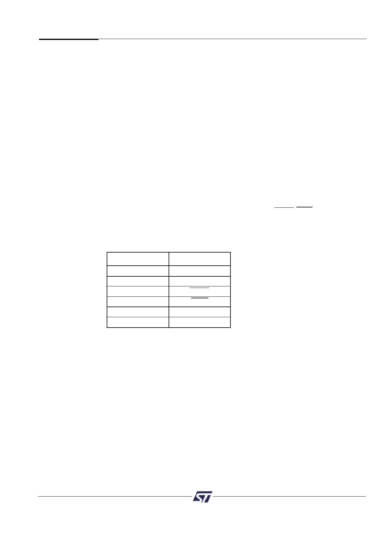
5.6 JTAG Port
In-System Programming can be performed through the JTAG pins on Port C. This serial
interface allows complete programming of the entire PSD813F1 device. A blank device can
be completely programmed. The JTAG signals (TMS, TCK, TSTAT, TERR, TDI, TDO) can
be multiplexed with other functions on Port C. Table 3 indicates the JTAG signals pin
assignments.
Table 3. JTAG Signals on Port C
Port C Pins
JTAG Signal
PC0
TMS
PC1
TCK
PC3
TSTAT
PC4
TERR
PC5
TDI
PC6
TDO
7
Share Link: 