M28F008 Просмотр технического описания (PDF) - Intel
Номер в каталоге
Компоненты Описание
производитель
M28F008 Datasheet PDF : 28 Pages
| |||
M28F008
erase and byte write circuitry Write cycles also inter-
nally latch addresses and data needed for byte write
or block erase operations With the appropriate com-
mand written to the register standard microproces-
sor read timings output array data access the intelli-
gent identifier codes or output byte write and block
erase status for verification
Interface software to initiate and poll progress of in-
ternal byte write and block erase can be stored in
any of the M28F008 blocks This code is copied to
and executed from system RAM during actual flash
memory update After successful completion of byte
write and or block erase code data reads from the
M28F008 are again possible via the Read Array
command Erase suspend resume capability allows
system software to suspend block erase to read
data and execute code from any other block
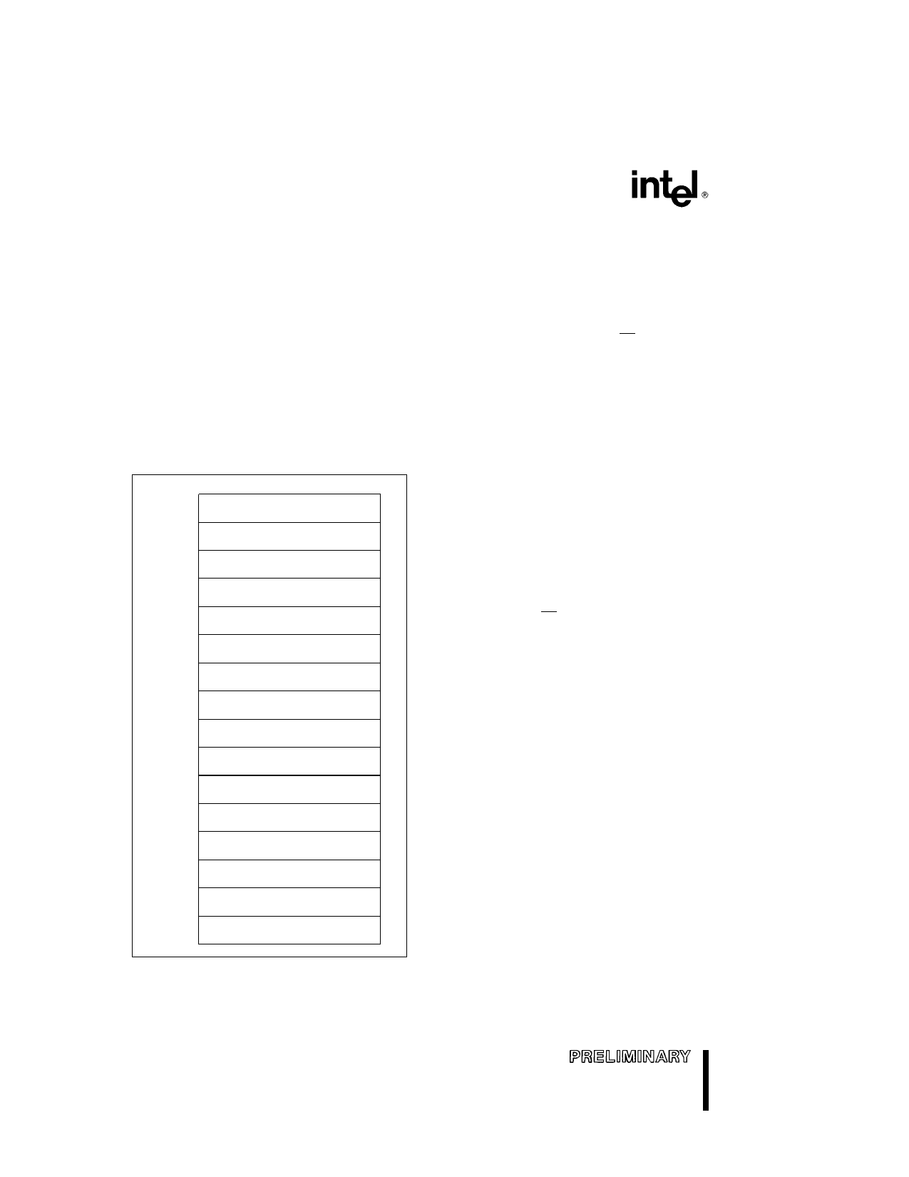
FFFFF
F0000
EFFFF
E0000
DFFFF
D0000
CFFFF
C0000
BFFFF
B0000
AFFFF
A0000
9FFFF
90000
8FFFF
80000
7FFFF
70000
6FFFF
60000
5FFFF
50000
4FFFF
40000
3FFFF
30000
2FFFF
20000
1FFFF
10000
0FFFF
00000
64 Kbyte Block
64 Kbyte Block
64 Kbyte Block
64 Kbyte Block
64 Kbyte Block
64 Kbyte Block
64 Kbyte Block
64 Kbyte Block
64 Kbyte Block
64 Kbyte Block
64 Kbyte Block
64 Kbyte Block
64 Kbyte Block
64 Kbyte Block
64 Kbyte Block
64 Kbyte Block
Figure 4 Memory Map
Command User Interface and Write
Automation
An on-chip state machine controls block erase and
byte write freeing the system processor for other
tasks After receiving the Erase Setup and Erase
Confirm commands the state machine controls
block pre-conditioning and erase returning progress
via the Status Register and RY BY output Byte
write is similarly controlled after destination address
and expected data are supplied The program and
erase algorithms of past Intel Flash memories are
now regulated by the state machine including pulse
repetition where required and internal verification
and margining of data
Data Protection
Depending on the application the system designer
may choose to make the VPP power supply switcha-
ble (available only when memory byte writes block
erases are required) or hardwired to VPPH When
VPP e VPPL memory contents cannot be altered
The M28F008 Command User Interface architecture
provides protection from unwanted byte write or
block erase operations even when high voltage is
applied to VPP Additionally all functions are dis-
abled whenever VCC is below the write lockout volt-
age VLKO or when RP is at VIL The M28F008 ac-
commodates either design practice and encourages
optimization of the processor-memory interface
The two-step byte write block erase Command User
Interface write sequence provides additional soft-
ware write protection
BUS OPERATION
Flash memory reads erases and writes in-system
via the local CPU All bus cycles to or from the flash
memory conform to standard microprocessor bus
cycles
Read
The M28F008 has three read modes The memory
can be read from any of its blocks and information
can be read from the intelligent identifier or Status
Register VPP can be at either VPPL or VPPH
The first task is to write the appropriate read mode
command to the Command User Interface (array in-
telligent identifier or Status Register) The M28F008
automatically resets to Read Array mode upon initial
device powerup or after exit from deep powerdown
The M28F008 has four control pins two of which
6
6
Share Link: 