PLL102-109XM Просмотр технического описания (PDF) - PhaseLink Corporation
Номер в каталоге
Компоненты Описание
производитель
PLL102-109XM Datasheet PDF : 10 Pages
| |||
Preliminary PLL102-109
Programmable DDR Zero Delay Clock Driver
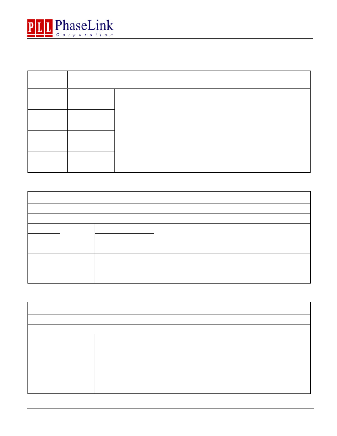
TABLE 3: Output Drive Strength Programming Summary:
Bit<2:0>
111
110
101
100
011
010
001
000
Programming Setting
+40%
+30%
+20%
+10%
Default
-10%
-20%
-30%
Setting applies to the following outputs
1. DDRA (CLK0, CLK1, CLK5)
2. DDRB (CLK2, CLK3, CLK4)
3. FBOUT
6. Byte 9: Buffer Drive Strength Control Register
Bit
Name
Default
Description
Bit 7
-
1
Reserved.
Bit 6
-
1
Reserved.
Bit 5
Bit <2>
Bit 4
DDRA
Strength
Bit <1>
Bit 3
Bit <0>
0
1
These three bits will program drive strength for CLK0, CLK1 and
CLK5 output clocks (see Table 3).
1
Bit 2
-
Bit 1
-
-
-
Reserved
-
-
Reserved
Bit 0
-
-
-
Reserved
7. Byte 10: Buffer Drive Strength Control Register
Bit
Name
Default
Description
Bit 7
-
1
Reserved.
Bit 6
-
1
Reserved.
Bit 5
Bit <2>
Bit 4
DDRC
Strength
Bit <1>
Bit 3
Bit <0>
0
1
These three bits will program drive strength for CLK2, CLK3 and
CLK4 output clocks (see Table 3).
1
Bit 2
-
Bit 1
-
-
-
Reserved
-
-
Reserved
Bit 0
-
-
-
Reserved
47745 Fremont Blvd., Fremont, California 94538 TEL (510) 492-0990 FAX (510) 492-0991
Rev 02/26/03 Page 6
Share Link: 