HI1276-EV Просмотр технического описания (PDF) - Intersil
Номер в каталоге
Компоненты Описание
производитель
HI1276-EV Datasheet PDF : 11 Pages
| |||
HI1276
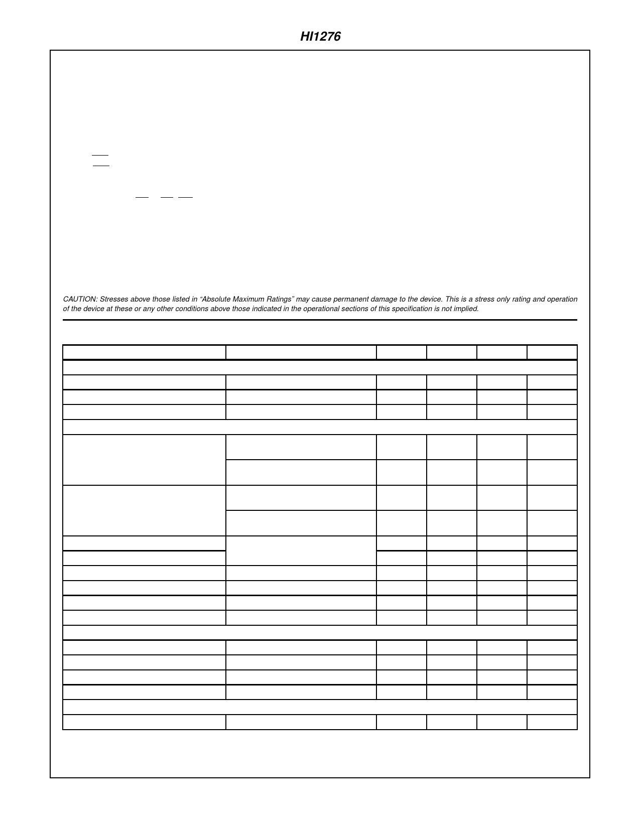
Absolute Maximum Ratings TA = 25oC
Supply Voltage (AVEE, DVEE) . . . . . . . . . . . . . . . . . . . -7V to +0.5V
Analog Input Voltage (VIN) . . . . . . . . . . . . . . . . . . . . . . -2.7 to +0.5V
Reference Input Voltage
VRT, VRB, VRM . . . . . . . . . . . . . . . . . . . . . . . . . . . AVEE to +0.5V
|VRT - VRB|. . . . . . . . . . . . . . . . . . . . . . . . . . . . . . . . . . . . . . . 2.5V
Digital Input Voltage
MINV, LINV . . . . . . . . . . . . . . . . . . . . . . . . . . . . . . . . -4V to +0.5V
CLK, CLK, . . . . . . . . . . . . . . . . . . . . . . . . . . . . . . .DVEE to +0.5V
|CLK-CLK | . . . . . . . . . . . . . . . . . . . . . . . . . . . . . . . . . . . . . . . 2.7V
VRM Pin Input Current (IVRM) . . . . . . . . . . . . . . . . . . -3mA to +3mA
Digital Output Current
(ID0 to ID7, IOR, ID0 to ID7, IOR) . . . . . . . . . . . . . -30mA to 0mA
Thermal Information
Thermal Resistance (Typical)
θJAoC/W θJCoC/W
CLCC Package . . . . . . . . . . . . . . . . . .
18
4
Maximum Junction Temperature . . . . . . . . . . . . . . . . . . . . . . 175oC
Maximum
Maximum
Storage Temperature Range (TSTG)
Lead Temperature (Soldering 10s) . .
.
.
.
.
.
.
.-65oC
......
to
.
150oC
300oC
Operating Conditions (Note 1)
Supply Voltage
MIN
AVEE, DVEE . . . . . . . . . . . . . . . . . . . . . . . -5.5V
AVEE - DVEE. . . . . . . . . . . . . . . . . . . . . . .-0.05V
AGND - DGND . . . . . . . . . . . . . . . . . . . . .-0.05V
Temperature Range (Note 5)
TC . . . . . . . . . . . . . . . . . . . . . . . . . . . . . . . -20oC
TYP
-5.2V
0V
0V
-
MAX
-4.95V
0.05V
0.05V
100oC
Reference Input Voltage
MIN TYP
VRT . . . . . . . . . . . . . . . . . . . . . . . . . . . . . -0.1V -2
VRB . . . . . . . . . . . . . . . . . . . . . . . . . . . . . -2.2V -2
Analog Input Voltage, VIN . . . . . . . . . . . . . . VRB -
MAX
0.1V
-1.8V
VRT
CAUTION: Stresses above those listed in “Absolute Maximum Ratings” may cause permanent damage to the device. This is a stress only rating and operation
of the device at these or any other conditions above those indicated in the operational sections of this specification is not implied.
Electrical Specifications TA = 25oC, AVEE = DVEE = -5.2V, VRT, VRTS = 0V, VRB, VRBS = -2V (Note 1)
PARAMETER
TEST CONDITIONS
MIN
TYP
MAX
SYSTEM PERFORMANCE
Resolution
-
8
-
Integral Linearity Error, INL
Differential Linearity Error, DNL
DYNAMIC CHARACTERISTICS
fC = 500 MSPS
fC = 500 MSPS
-
±0.3
±0.7
-
±0.3
±0.5
Signal to Noise and Distortion Ratio, SINAD
= R-----M-----S------N--R--o--M-i--s--S-e----+-S----iD-g----ni--s-a--t-l--o---r---t--i--o----n-
Error Rate
Differential Gain Error, DG
Differential Phase Error, DP
Input = 1kHz, Full Scale
fC = 500 MSPS
Input = 100MHz, Full Scale
fC = 500 MSPS
Input = 100MHz, Full Scale
Error > 16 LSB, fC = 400 MSPS
Input = 125MHz, Full Scale
Error > 16 LSB, fC = 500 MSPS
NTSC 40 IRE Mod.
Ramp, fC = 500 MSPS
-
46
-
-
37
-
-
10-11
10-9
-
10-8
10-6
-
1.0
-
-
0.5
-
Overrange Recovery Time
-
1.0
-
Maximum Conversion Rate, fC
Aperture Jitter, tAJ
Sampling Delay, tDS
ANALOG INPUT
Input = 150MHz
Input = 150MHz
500
-
-
-
11
-
0.2
0.8
1.5
Analog Input Capacitance, CIN
Analog Input Resistance, RIN
Input Bias Current, IIN
Full Scale Input Bandwidth
REFERENCE INPUTS
VIN = 1V + 0.07VRMS
VIN = -1V
VIN = 2VP-P
-
20
-
30
70
-
-
-
850
300
-
-
Reference Resistance, RREF
70
110
160
UNITS
Bits
LSB
LSB
dB
dB
TPS
(Note 3)
TPS
(Note 3)
%
Degree
ns
MSPS
ps
ns
pF
kΩ
µA
MSPS
Ω
4-3
Share Link: 