HI2302(1997) Просмотр технического описания (PDF) - Intersil
Номер в каталоге
Компоненты Описание
производитель
HI2302 Datasheet PDF : 16 Pages
| |||
HI2302
Electrical Specifications Measurement Circuits (Continued)
2.5V
0.5V
VDD
VRT
VIN
VRB
CLK
OE
GND
IOL
+
VOL -
2.5V
0.5V
VDD
VRT
VIN
VRB
CLK
OE
GND
IOH
+
VOH -
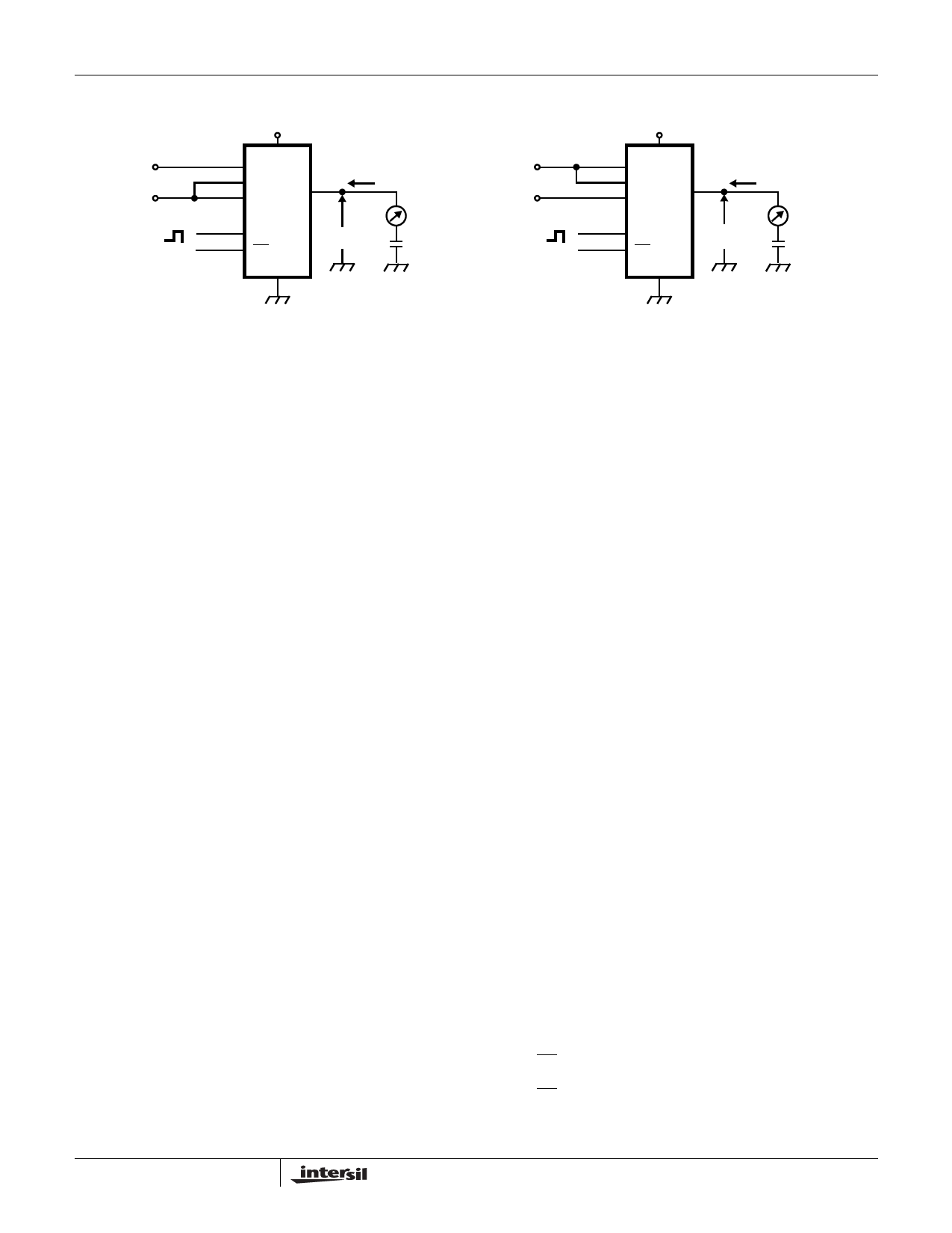
FIGURE 6. DIGITAL OUTPUT CURRENT TEST CIRCUIT
Operation (See Block diagram and Timing Chart II)
Notes On Operation
• The HI2302 is a two-step parallel system A/D converter
featuring a 4-bit upper comparator block and two lower
comparator blocks of 4-bit each. The reference voltage
that is equal to the voltage between VRT - VRB/16 is
constantly applied to the upper 4-bit comparator block.
Voltage that corresponded to the upper data is fed through
the reference supply to the lower 4-bit comparator block.
Voltage that corresponded to the upper data is fed through
the reference supply to the lower 4-bit comparator block.
VRTS and VRBS pins serve for the self generation of VRT
(reference voltage top) and VRB (reference voltage bot-
tom), and they are also used as the sense pins as shown
in the Application Circuit examples Figures 10 and 11.
• This IC uses an offset cancel type comparator which
operates synchronously with an external clock. It features
the following operating modes which are respectively indi-
cated on the Timing Chart II with S, H, C symbols. That is
input sampling (auto zero) mode, input hold mode and
comparison mode.
• The operation of respective parts is as indicated in the
Timing Chart II. For instance, input voltage VI (1) is sam-
pled with the falling edge of the external clock (1) by
means of the upper comparator block and the lower
comparator A block.
The upper comparator block finalizes comparison data MD
(1) with the rising edge of the external clock (2).
Simultaneously the reference supply generates the lower
reference voltage RV (1) that corresponded to the upper
results. The lower comparator A Block finalizes compari-
son data LD (1) with the rising edge of the external clock
(3). MD (1) and LD (1) are combined and output as Out (1)
with the rising edge of the external clock (4). Accordingly
there is a 2.5 clock delay from the analog input sampling
point to the digital data output.
• VDD , VSS
To reduce noise effects, separate the analog and digital
systems close to the device. For both the digital and analog
VDD pins, use a ceramic capacitor of about 0.1µF set as
close as possible to the pin to bypass to the respective
GNDs.
• Analog Input
Compared with the flash type A/D converter, the input
capacitance of the analog input is rather small. However, it
is necessary to conduct the drive with an amplifier featur-
ing sufficient band and drive capability. When driving with
an amplifier of low output impedance, parasitic oscillation
may occur. That may be prevented by insetting a resis-
tance of about 33Ω in series between the amplifier output
and A/D input. When the VIN signal of pin No. 21 is moni-
tored, the kickback noise of clock is. However, this has no
effect on the characteristics of A/D conversion.
• Clock Input
The clock line wiring should be as short as possible also,
to avoid any interference with other signals, separate it
from other circuits.
• Reference Input
Voltage VRT to VRB is compatible with the dynamic range
of the analog input. Bypassing VRT and VRB pins to GND,
by means of a capacitor about 0.1µF, stable characteris-
tics are obtained. By shorting VDD and VRTS, VSS and
VRBS respectively, the self-bias function that generates
VRT = about 2.5V and VRB = about 0.6V, is activated.
• Timing
Analog input is sampled with the falling edge of CLK and
output as digital data synchronized with a delay of 2.5
clocks and with the following rising edge. The delay from
the clock rising edge to the data output is about 9ns
(DVDD = 5V).
• OE Pin
Pins 1 to 8 (D0 to D7) are in the output mode by leaving
OE open or connecting it to DVSS, and they are in the high
impedance mode by connecting it to DVDD.
4-10
Share Link: 