ADC-305-3 Просмотр технического описания (PDF) - DATEL Data Acquisition products
Номер в каталоге
Компоненты Описание
производитель
ADC-305-3 Datasheet PDF : 6 Pages
| |||
®
®
ADC-305
These values may differ from one device to another. Voltage
changes on the +5V supply have a direct influence on the
performance of the device. The use of external references is
recommended for applications sensitive to gain error.
External Reference Mode
Tie VRB to AGND, and apply +2V to VRT to use at 0 to +2V
input voltage range. The reference resistance between VRB
and VRT is about 300 ohms. It is important to make the
output impedance of the reference source small enough
while, at the same time, keeping sufficient drive capacity.
Insert a 0.1µF bypass ceramic chip capacitor between VRT
and GND to minimize the effect of the 20MHz clock
running nearby. See Figure 5.
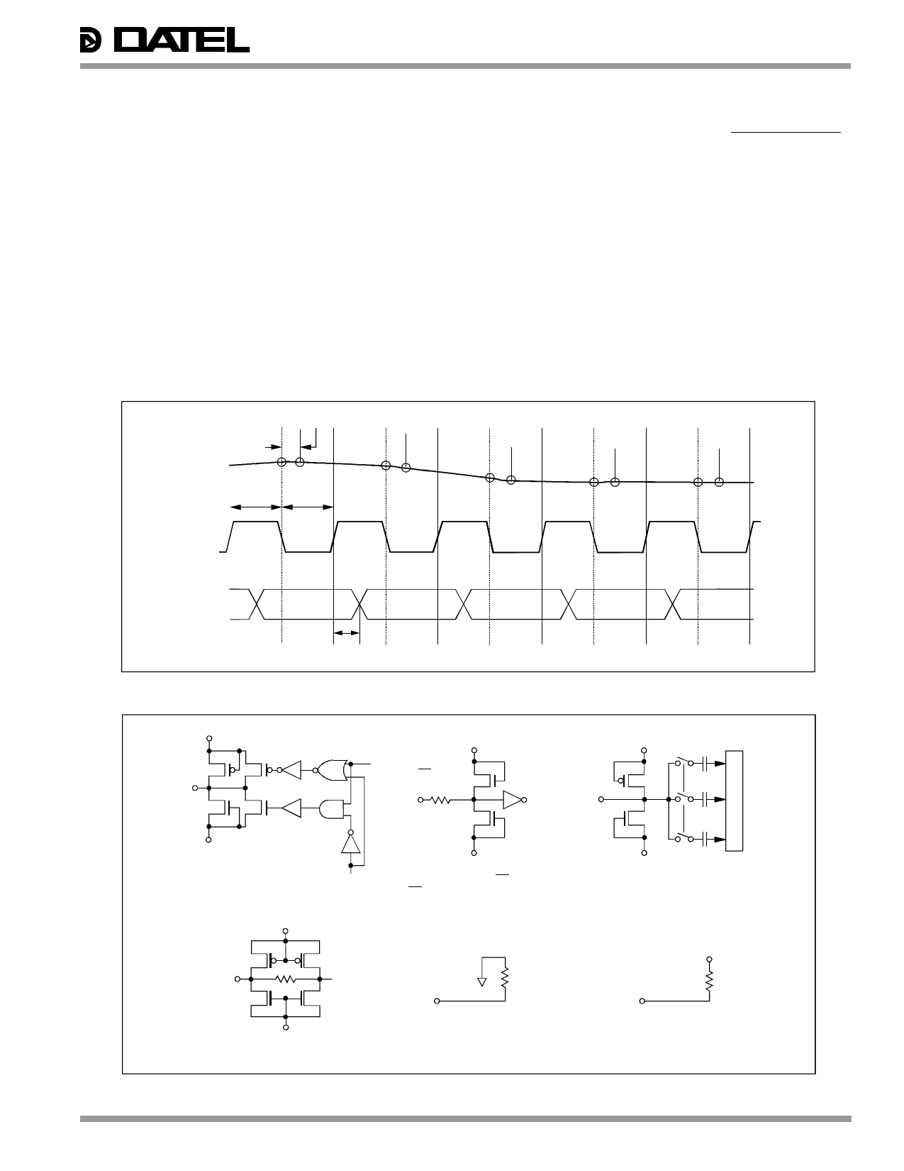
5. Logic inputs are CMOS compatible. Normally a series 74HC
is used as a driver. It is recommended to pull up to +5V if
the device is driven with TTL.
6. The start convert (A/D CLK) pulse can be a 50% duty cycle
clock. Both TPW1 and TPW0 are 25ns minimum. A slightly
longer TPW1 will improve linearity of the system for higher
frequency input signals.
7. The digital data outputs are 3-state and TTL compatible. To
enable the 3-state outputs, connect the OUTPUT ENABLE
(pin 1) to GND. To disable, connect it to +5V. It is
recommended that the data outputs be latched and buffered
through output registers.
8. Maximum 30ns (18ns typical) after the rising edge of the
Nth conversion pulse, the result of the (N-3) conversion can
be obtained. Data is stored firmly in an output register, such
as an 74LS574, using the rising edge of a start convert
pulse as a trigger. The (N–4) data is stored in this case. See
the timing diagrams, Figure 2 and 4.
9. The 20MHz sampling rate is guaranteed. It is not
recommended to use this device at sampling rates slower
than 500kHz because the droop characteristics of the
internal sample and holds will then exceed the limit
required to maintain the specified accuracy of the device.
Ta
ANALOG
INPUT
N
N+1
TPW1
TPW0
N+2
N+3
N+4
CLOCK
DATA
N-3
N-2
N-1
OUTPUT
N
N+1
Td= 30ns max.
Figure 2. Timing Diagram
+DVS
+DGND
Digital Output Circuit, Bit1 through Bit 8
+AVS
VRT
17
VRB
23
AGND
Voltage Reference (VRT,VRB)
Equivalent Circuit
+DVS
+AVS
OE
VIN
19
A/D CLK
DGND
Equivalent Circuit for OE and A/D CLK
OE - Low data is output when high digital
output pins turn to high impedance.
AGND
Analog Input
VRBS AGND
22
Generates +0.6V
when shorted with VB
+AVS
VRTS
16
Generates +2.6V
when shorted with VT
Figure 3. Equivalent Circuits
3
Share Link: 