HI3276 Просмотр технического описания (PDF) - Intersil
Номер в каталоге
Компоненты Описание
производитель
HI3276 Datasheet PDF : 16 Pages
| |||
HI3276
TABLE 1. A/D CODE
INV
1
0
VIN STEP D7
D0 D7
D0
VRT
255 1 1 1 1 1 1 1 1 0 0 0 0 0 0 0 0
254 1 1 1 1 1 1 1 0 0 0 0 0 0 0 0 1
•
•
•
•
•
•
•
•
•
VRM2
128 1 0 0 0 0 0 0 0 0 1 1 1 1 1 1 1
127 0 1 1 1 1 1 1 1 1 0 0 0 0 0 0 0
•
•
•
•
•
•
•
•
•
1 0000000111111110
VRB
0 0000000011111111
Notes on Operation
• The HI3276 is a high-speed A/D converter which is capable
of TTL, ECL and PECL level clock input. Characteristic
impedance should be properly matched to ensure optimum
performance during high-speed operation.
• The power supply and grounding have a profound influence
on converter performance. The power supply and
grounding method are particularly important during high-
speed operation. General points for caution are as follows:
- The ground pattern should be as large as possible. It is
recommended to make the power supply and ground
patterns wider at an inner layer using a multi-layer board.
- To prevent interference between AGND and DGND and
between AVCC and DVCC, make sure the respective
patterns are separated. To prevent a DC offset in the
power supply pattern, connect the AVCC and DVCC lines
Test Circuits
4V
1.95V
2V
VRT
VIN
VRB
5V
5V
A ICC
AVCC
DVCC1
DVCC2
A IEE
DGND3
CLK/E
5MHz PECL
DGND2
DGND1
AGND
DVEE3
FIGURE 4. CURRENT CONSUMPTION MEASUREMENT
CIRCUIT
at one point each, via a ferrite-bead filter. Shorting the
AGND and DGND patterns in one place immediately
under the A/D converter improves A/D converter
performance.
- Ground the power supply pins (AVCC, DVCC1, DVCC2,
DVEE3) as close to each pin as possible with a 0.1µF or
larger ceramic chip capacitor. (Connect the AVCC pin to
the AGND pattern and the DVCC1, DVCC2 , DVEE3 pins
to the DGND pattern).
- The digital output wiring should be as short as possible. If
the digital output wiring is long, the wiring capacitance
will increase, deteriorating the output slew rate and
resulting in reflection to the output waveform since the
original output slew rate is quite fast.
• The analog input pin VIN has an input capacitance of
approximately 10pF. To drive the A/D converter with proper
frequency response, it is necessary to prevent performance
deterioration due to parasitic capacitance or parasitic
inductance by using a large capacity drive circuit; keeping
wiring as short as possible, and using chip parts for
resistors and capacitors, etc.
• The VRT and VRB pins must have adequate bypass to
protect them from high-frequency noise. Bypass them to
AGND with approximately 1µF tantal capacitor and, 0.1µF
capacitor. At this time, approximately DGND3 - 1.2V voltage
is generated. However, this is not recommended for use as
threshold voltage VBB as it is too weak.
• The TTL output high level is clamped to approximately 2.8V
in the IC. This makes it possible to directly interface with
3.3V CMOS ICs.
When the digital input level is PECL level, ***/E pins should
be used and ***/T pins left open. When the digital input level
is TTL, ***/T pins should be used and III/E pins left open.
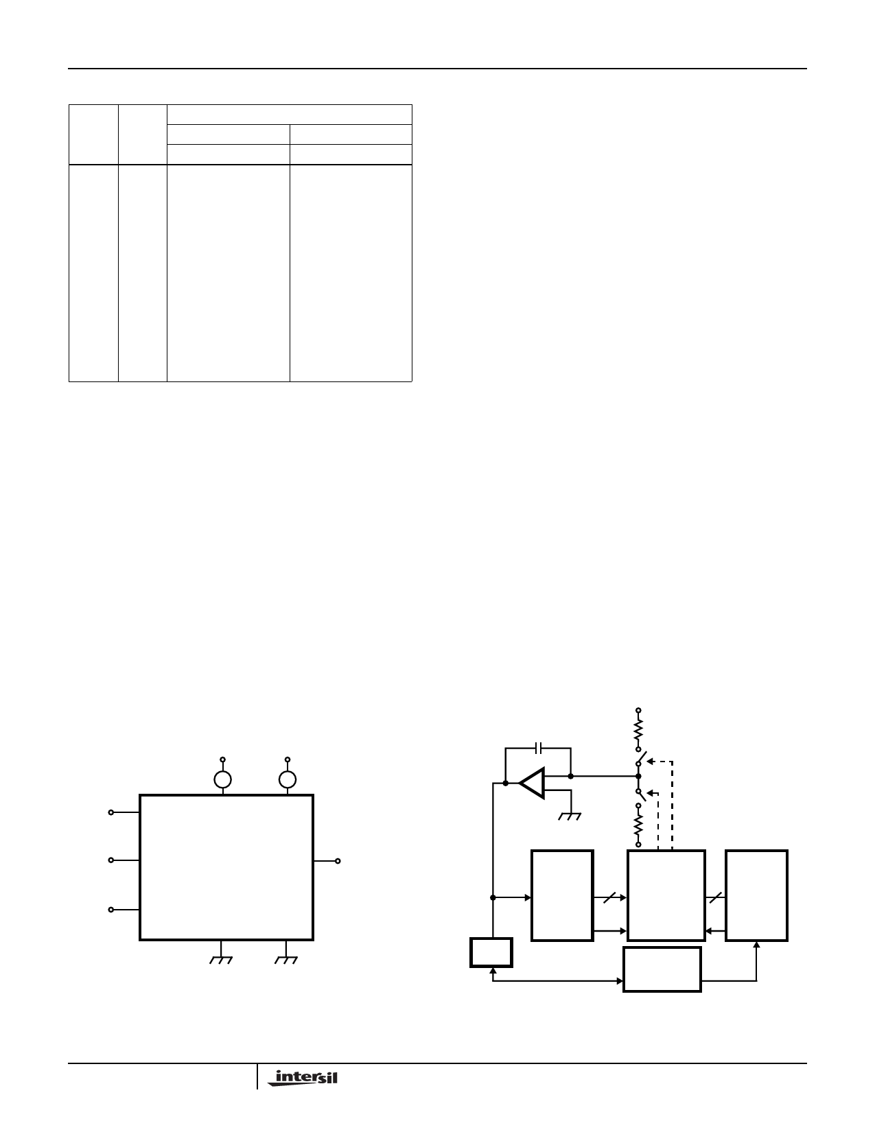
+V
S2
-
+
S1 S1: ON WHEN A < B
S2: ON WHEN A > B
VIN
DVM
HI3276
-V
A<B A>B
COMPARATOR
8
A8 B8
TO TO
8
BUFFER
A1 B1
A0 B0
“0”
“1”
CONTROLLER
000...00
TO
111..10
FIGURE 5. INTEGRAL LINEARITY ERROR/DIFFERENTIAL
LINEARITY ERROR MEASUREMENT CIRCUIT
9
Share Link: 