PI90LVB010 Просмотр технического описания (PDF) - Pericom Semiconductor
Номер в каталоге
Компоненты Описание
производитель
PI90LVB010 Datasheet PDF : 9 Pages
| |||
PI90LVB010
Single Bus LVDS Transceiver
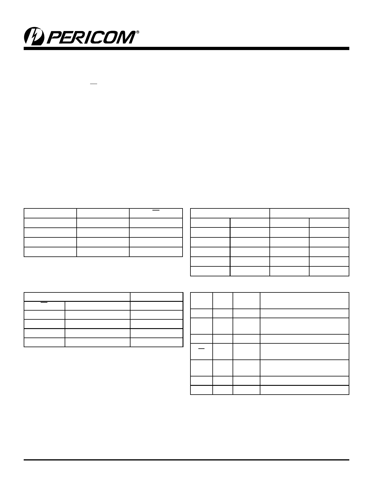
Absolute Maximum Ratings(1,2)
Supply Voltage (VCC) ...........................................................6.0V
Enable Input Voltage (DE, RE)..................–0.3V to (VCC +0.3V)
Driver Input Voltage (DIN)........................–0.3V to (VCC +0.3V)
Receiver Output Voltage (ROUT) ...............–0.3V to (VCC +0.3V)
Bus Pin Voltage (DO/RI±) ................................... –0.3V to +3.9V
Driver Short Circuit .................................................... Continuous
ESD (HBM 1.5kΩ, 100pF)................................................ >10kV
Maximum Package Power Dissipation at 20°C
SOIC ............................................................................1025mW
Derate SOIC Package ............................................... 8.2mW/°C
Storage Temperature Range ...............................–65°C to +150°C
Lead Temperature Range (Soldering, 4s) ......................... +260°C
Recommended Operating Conditions
Min. Max.
Supply Voltage (VCC)
Receiver Input Voltage
Operating Free-Air Temperature
3.0
3.6
0.0
2.9
–40 +85
Units
V
V
°C
Note:
Stresses greater than those listed under Absolute Maximum Ratings may cause permanent damage to the device. This is a stress rating only and func-
tional operation of the device at these or any other conditions above those indicated in the operational sections of this specification is not implied.
Exposure to absolute maximum rating conditions for extended periods may affect reliability.
Functional Mode
Mode Select
DE
RE
Driver Mode
H
H
Receiver Mode
L
L
3-State Mode
L
H
Loop Back Mode
H
L
Receiver Mode
Inputs
Outputs
RE
(RE+) - (RI-)
ROUT
L
L (< -100mV)
L
L
H (> + 100mV)
H
L
100mV > & >-100mV
?
H
X
Z
Notes:
1. H = High, L = Low, Z = High Impedance, X = High or Low
Transmitter Mode
Inputs
DE
DI
H
L
H
H
H
2 > & > 0.8
L
X
H
Open
Outputs
DO+
DO-
L
H
H
L
X
X
Z
Z
L
H
Pin Description
Pin Pin# Inputs/
Name
Outputs
Description
DIN
2
DO±
RI±
6, 7
I TTL Driver Input
I/O
LVDS Driver Outputs/
LVDS Receiver Inputs
ROUT 3
O TTL Receiver Outputs
RE
5
I
Receiver Enable TTL Input
(Active Low)
DE
1
I
Driver Enable TTL Input
(Active High)
GND 4
NA Ground
VCC
8
NA Power Supply
2
PS8662A
09/03/04
Share Link: 