PI6C102 Просмотр технического описания (PDF) - Pericom Semiconductor
Номер в каталоге
Компоненты Описание
производитель
PI6C102 Datasheet PDF : 11 Pages
| |||
PI6C102
111222333444555666777888999000111222333444555666777888999000111222333444555666777888999000111222111222333444555666777888999000111222333444555666777888999000111222333444555666777888999000111222111222333444555666777888999000111222333444555666777888999P000111r222e333c444555i666s777i888o999n000111222C111222l333o444c555666k777888S999000y111n222333t444h555666e777s888i999z000111e222r333444f555o666777r888M999000111o222111b222333i444le555666P777888C999000s111222
Power Management Timing
Signal
Signal State
Latency
No. of rising edges of free running PCICLK
CPU_STOP#
0 (disabled)
1
1 (enabled)
1
PCI_STOP#
0 (disabled)
1
1 (enabled)
1
PWR_DWN# 1 (normal operation)
3ms
0 (power down)
2 max.
Notes:
1. Clock on/off latency is defined as the number of rising edges of free running PCICLKs
between when the clock disable goes low/high to when the first valid clock comes out of
the device.
2. Power-up latency is from when PWR_DWN# goes inactive (HIGH) to when the first valid
clocks are driven from the device.
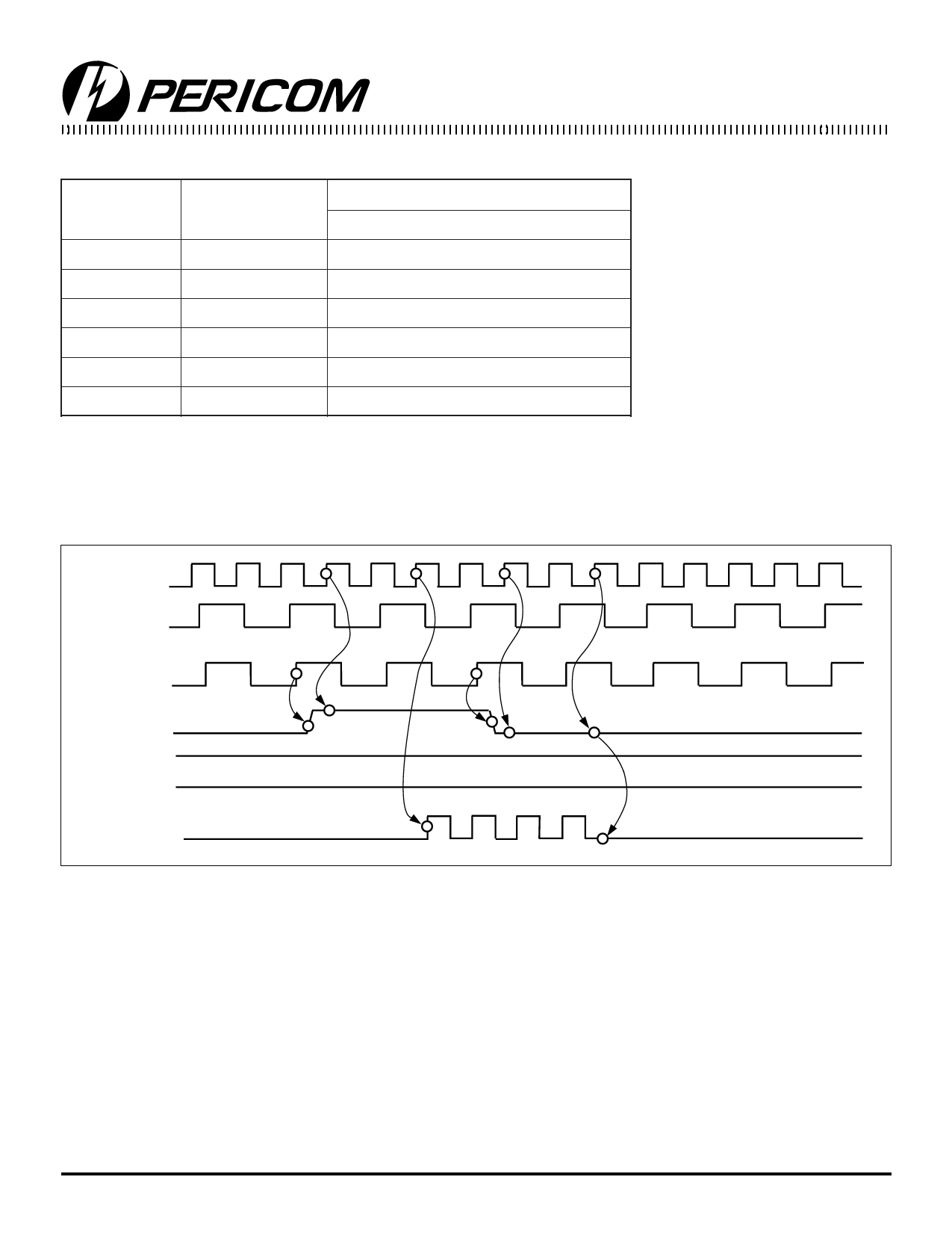
CPUCLK
(Internal)
CPUCLK
(Internal)
PCICLK_F
(Free-running)
CPU_STOP#
PCI_STOP#
PWR_DWN#
CPUCLK
(External)
CPU_STOP# Timing Diagram
Notes:
1. All timing is referenced to the CPUCLK.
2. The Internal label means inside the chip and is a reference only.
3 CPU_STOP# is an input signal that must be made synchronous to the free running PCI_F.
4. ON/OFF latency shown in the diagram is 2 CPU clocks.
5. All other clocks continue to run undisturbed.
6. PWR_DWN# and PCI_STOP# are shown in a HIGH state.
7. Diagrams shown with respect to 66 MHz. Similar operation as CPU = 100 MHz.
CPU_STOP# is an input signal used to turn off the CPU clocks for
low power operation. CPU_STOP# is asserted asynchronously by
the external clock control logic with the rising edge of free running
PCI clock and is internally synchronized to the external PCICLK_F
output. All other clocks continue to run while the CPU clocks are
disabled. The CPU clocks are always stopped in a LOW state and
started guaranteeing that the high pulse width is a full pulse. CPU
clock on latency is 2 or 3 CPU clocks and CPU clock off latency
is 2 or 3 CPU clocks.
3
PS8164A
09/29/00
Share Link: 