PDIUSBP11A Просмотр технического описания (PDF) - Philips Electronics
Номер в каталоге
Компоненты Описание
производитель
PDIUSBP11A Datasheet PDF : 12 Pages
| |||
Philips Semiconductors
Universal Serial Bus transceiver
Product specification
PDIUSBP11A
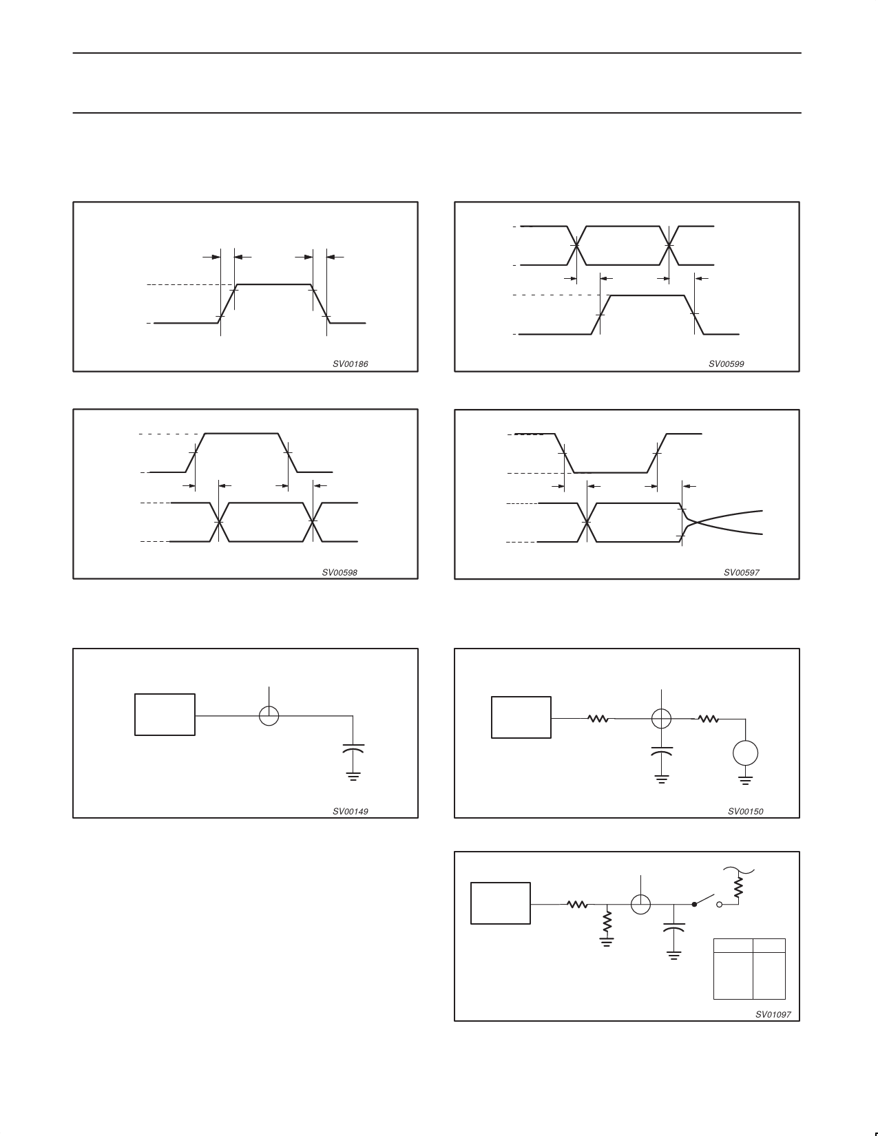
AC WAVEFORMS
VOL and VOH are the typical output voltage drops that occur with the
output load. (VCC never goes below 3.0V).
tRISE
tFALL
VOH
VOL
90%
90%
10%
10%
SV00186
Waveform 1. Rise and Fall Times
2.7V
GND
INPUT
D+
D–
1.5V
tPLH
VCR
1.5V
tPHL
VCR
SV00598
Waveform 2. VPO, VMO/FSEO to D+/D–
TEST CIRCUITS AND WAVEFORMS
Test Point
D.U.T.
25pF
SV00149
Load for VM/VP and RCV
D+
D–
VOH
VOL
VCR
tPLH
1.5V
VCR
tPHL
2.0V
1.0V
1.5V
SV00599
Waveform 3. D+/D– to RCV, VP/VM
2.7V
0V
OE#
VOH
VOL
D+/D–
1.5V
tPZH
tPZL
0.5VCC
VM
1.5V
tPHZ
tPLZ
VOH–0.3
VOL+0.3
0.5VCC
Waveform 4. OE# to D+/D–
SV00597
24Ω
D.U.T.
V = 0 for tPZH, tPHZ
V = VCC for tPZL, tPLZ
Test Point
500Ω
50pF
V
+
–
SV00150
Load for Enable and Disable Times
D.U.T.
Test Point
24Ω
VCC
S1
1.5kΩ*
15kΩ
CL
CL = 50pF, Full Speed
CL = 200pF, Low Speed (Min Timing)
CL = 600pF, Low Speed (Max Timing)
* 1.5KΩ on D– (Low Speed) or D+ (Full Speed) Only
Load for D+/D–
Test
S1
D–/LS close
D+/LS open
D–/FS open
D+/FS close
SV01097
1999 Jun 04
7
Share Link: 