PCF2119VU-2-F2 Просмотр технического описания (PDF) - NXP Semiconductors.
Номер в каталоге
Компоненты Описание
производитель
PCF2119VU-2-F2 Datasheet PDF : 79 Pages
| |||
NXP Semiconductors
PCF2119x
LCD controllers/drivers
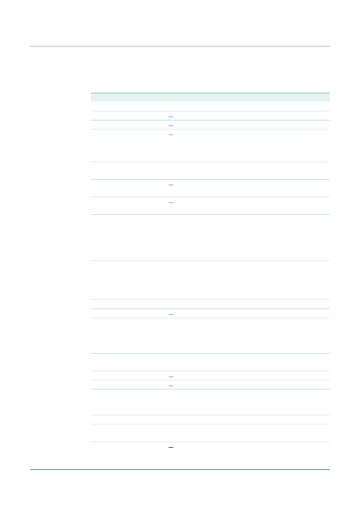
7.2 Pin description
Table 3.
Symbol
VDD1
VDD2
VDD3
E
Pin description
Pin
1 to 6
7 to 14
15 to 18
19
T1 and T2 20 and 21
VSS1
22 to 29
VSS2
30 to 35
VLCDSENSE
36
VLCDOUT
37 to 43
VLCDIN
dummy
R8 to R1,
R17,
R17DUP,
R18,
R9 to R16
C80 to C41,
C40 to C1
dummy
SCL
T3
44 to 49
50
51 to 58,
59,
100
141,
142 to 149
60 to 99,
101 to 140
150
151 and 152
153
POR
PD
SDA
154
155
156 and 157
Description
supply voltage 1 (logic)
[1] supply voltage 2 (for high voltage generator)
[1] supply voltage 3 (for high voltage generator)
[2] data bus clock input
• set HIGH to signal the start of a read or write operation
• data is clocked in or out of the chip on the negative edge
of the clock
test pins
• must be connected to VSS1
[3] ground supply voltage 1
• for all circuits, except of high voltage generator
[3] ground supply voltage 2
• for high voltage generator
input for voltage multiplier regulation circuitry and for the bias
level generation
• if VLCD is generated internally then this pin must be
connected to VLCDOUT and VLCDIN
• if VLCD is generated externally then this pin must be
connected to VLCDIN only
VLCD output
• if VLCD is generated internally then this pin must be
connected to VLCDIN and to VLCDSENSE
• if VLCD is generated externally then this pin must be left
open-circuit
input for LCD bias level generator
[4] -
LCD row driver output
• R17 has two pins: R17 and R17DUP
• R17 and R18 drive the icons
LCD column driver output
[4] -
[5] I2C-bus serial clock input
test pin
• open-circuit
• not user accessible
external Power-On Reset (POR) input
power-down mode select
• for normal operation pin PD must be LOW
[5] I2C-bus serial data input/output
PCF2119X_5
Product data sheet
Rev. 05 — 13 August 2009
© NXP B.V. 2009. All rights reserved.
5 of 79
Share Link: 