PCF2113AU Просмотр технического описания (PDF) - Philips Electronics
Номер в каталоге
Компоненты Описание
производитель
PCF2113AU Datasheet PDF : 72 Pages
| |||
Philips Semiconductors
LCD controllers/drivers
Product specification
PCF2113x
7 FUNCTIONAL DESCRIPTION
7.1 LCD supply voltage generator
The LCD supply voltage may be generated on-chip. The
VLCD generator is controlled by two internal 6-bit registers:
VA and VB. The nominal LCD operating voltage at room
temperature is given by the relationship:
VOP(nom) = (integer value of register × 0.08) + 1.82
7.1.1 PROGRAMMING RANGES
Programmed value: 1 to 63. Voltage: 1.90 to 6.86 V.
Tref = 27 °C.
Values producing more than 6.5 V at operating
temperature are not allowed. Operation above this
voltage may damage the device. When programming the
operating voltage the VLCD tolerance and temperature
coefficient must be taken into account.
Values below 2.2 V are below the specified operating
range of the chip and are therefore not allowed.
Value 0 for VA and VB switches the generator off
(i.e. VA = 0 in character mode, VB = 0 in icon mode).
Usually register VA is programmed with the voltage for
character mode and register VB with the voltage for icon
mode.
When VLCD is generated on-chip the VLCD pins should be
decoupled to VSS with a suitable capacitor.
The generated VLCD is independent of VDD and is
temperature compensated. When the VLCD generator and
the direct mode are switched off, an external voltage may
be supplied at connected pins VLCD1 and VLCD2. VLCD1 and
VLCD2 may be higher or lower than VDD2.
During direct mode (program DM register bit) the internal
VLCD generator is turned off and the VLCD2 output voltage
is directly connected to VDD2. This reduces the current
consumption during icon mode and Mux 1 : 9 (depending
on VDD2 value and LCD liquid properties).
The VLCD generator ensures that, as long as VDD is in the
valid range (2.2 to 4 V), the required peak voltage
VOP = 6.5 V can be generated at any time.
7.2 LCD bias voltage generator
The intermediate bias voltages for the LCD display are
also generated on-chip. This removes the need for an
external resistive bias chain and significantly reduces the
system current consumption. The optimum value of VLCD
depends on the multiplex rate, the LCD threshold voltage
(Vth) and the number of bias levels. Using a 5-level bias
scheme for 1 : 18 maximum rate allows VLCD < 5 V for
most LCD liquids. The intermediate bias levels for the
different multiplex rates are shown in Table 1. These bias
levels are automatically set to the given values when
switching to the corresponding multiplex rate.
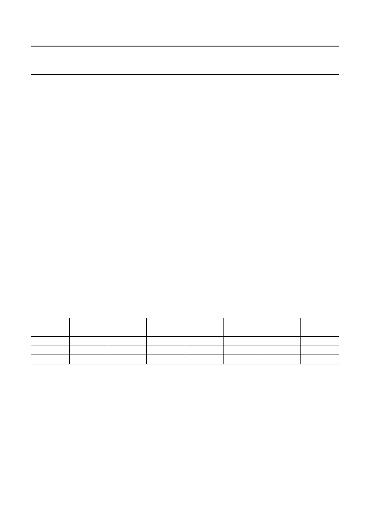
Table 1 Bias levels as a function of multiplex rate; note 1
MULTIPLEX NUMBER
RATE OF LEVELS
V1
V2
V3
V4
V5
V6
1 : 18
5
VLCD
3/4
1/2
1/2
1/4
VSS
1:9
5
VLCD
3/4
1/2
1/2
1/4
VSS
1:2
4
VLCD
2/3
2/3
1/3
1/3
VSS
Note
1. The values in the table are given relative to VLCD − VSS, e.g. 3/4 means 3/4 × (VLCD − VSS).
2001 Dec 19
9
Share Link: 