PCF2113AU Просмотр технического описания (PDF) - Philips Electronics
Номер в каталоге
Компоненты Описание
производитель
PCF2113AU Datasheet PDF : 72 Pages
| |||
Philips Semiconductors
LCD controllers/drivers
Product specification
PCF2113x
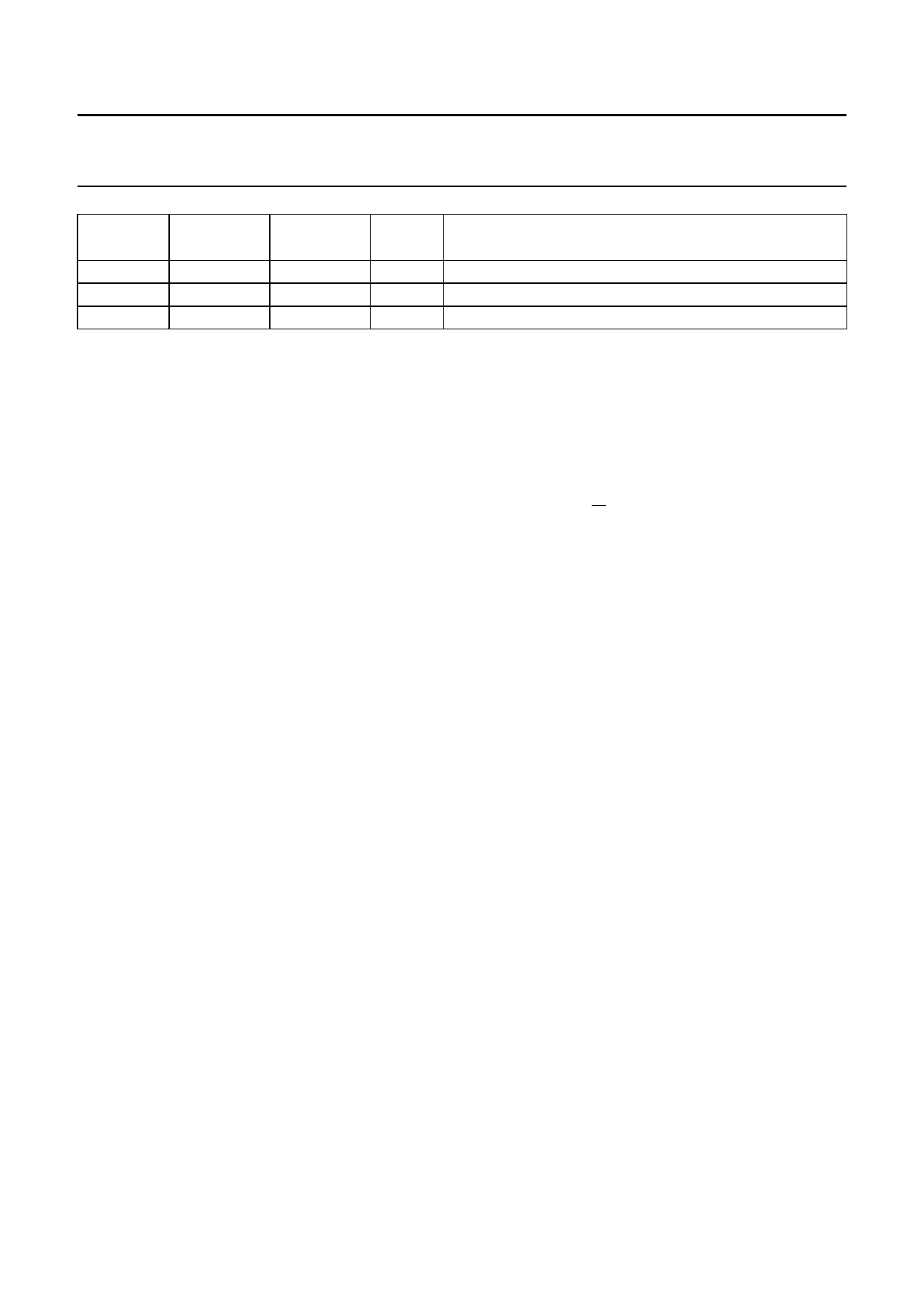
SYMBOL
PIN
PAD(1)
PCF2113DH PCF2113XU
TYPE
DESCRIPTION
DB0
99
108
I/O 8-bit bidirectional data bus bit 0
VDD2
VDD3
100
109
P
supply voltage 2 for VLCD generator; note 6
−
110
P
supply voltage 3 for VLCD generator; notes 3 and 6
Notes
1. Bonding pad location information is given in Chapter 17.
2. When the on-chip oscillator is used this pad must be connected to VDD1.
3. In the LQFP100 version this signal is connected internally and can not be accessed at any pin.
4. When the I2C-bus is used, the parallel interface pin E must be LOW. In the I2C-bus read mode DB7 to DB0 should
be connected to VDD1 or left open-circuit.
When the parallel bus is used, the pins SCL and SDA must be connected to VSS1 or VDD1; they must not be left
open-circuit.
When the 4-bit interface is used without reading out from the PCF2113x (R/W is set permanently to logic 0), the
unused ports DB0 to DB4 can either be set to VSS1 or VDD1 instead of leaving them open-circuit.
5. DB7 may be used as the busy flag, signalling that internal operations are not yet completed. In 4-bit operations the
four higher order lines DB7 to DB4 are used; DB3 to DB0 must be left open-circuit except for I2C-bus operations
(see note 4).
6. VDD2 and VDD3 should always be equal.
7. When VLCD is generated internally, pins VLCD1, VLCD2 and VLCDSENSE must be connected together. When external
VLCD is supplied, pin VLCD2 should be left open-circuit to avoid any stray current, pins VLCD1 and VLCDSENSE must be
connected together.
2001 Dec 19
7
Share Link: 