PCF2113AU Просмотр технического описания (PDF) - Philips Electronics
Номер в каталоге
Компоненты Описание
производитель
PCF2113AU Datasheet PDF : 72 Pages
| |||
Philips Semiconductors
LCD controllers/drivers
Product specification
PCF2113x
10 INTERFACES TO MICROCONTROLLER
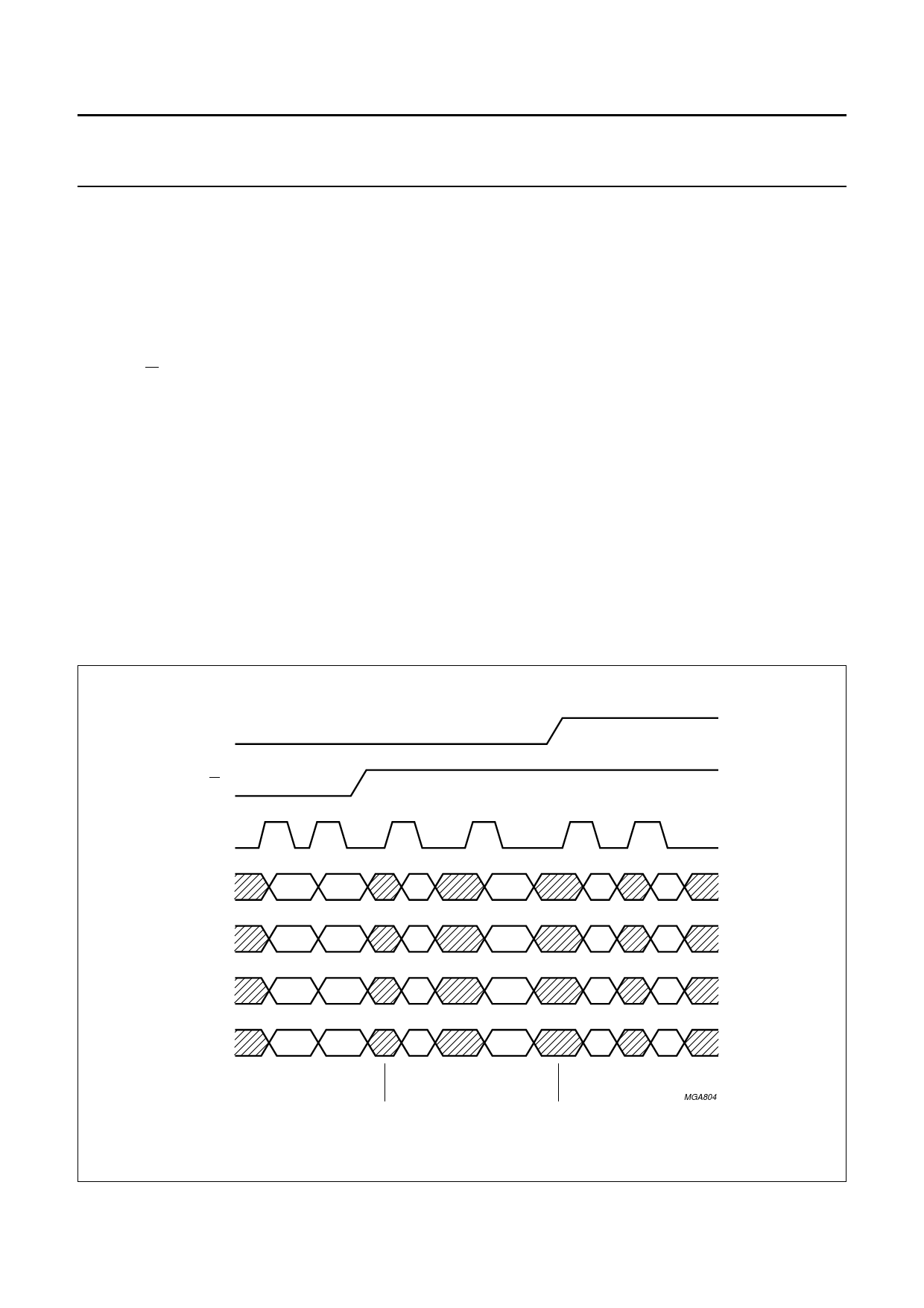
10.1 Parallel interface
The PCF2113x can send data in either two 4-bit operations
or one 8-bit operation and can thus interface to 4-bit or
8-bit microcontrollers.
In 8-bit mode data is transferred as 8-bit bytes using the
8 data lines DB7 to DB0. Three further control lines E,
RS and R/W are required (see Chapter 6).
In 4-bit mode data is transferred in two cycles of 4 bits
each using pins DB7 to DB4 for the transaction.
The higher order bits (corresponding to DB7 to DB4 in
8-bit mode) are sent in the first cycle and the lower order
bits (DB3 to DB0 in 8-bit mode) in the second cycle. Data
transfer is complete after two 4-bit data transfers. It should
be noted that two cycles are also required for the busy flag
check. 4-bit operation is selected by instruction, see
Figs 17 to 19 for examples of bus protocol.
In 4-bit mode, pins DB3 to DB0 must be left open-circuit.
They are pulled up to VDD internally.
10.2 I2C-bus interface
The I2C-bus is for bidirectional, two-line communication
between different ICs or modules. The two lines are the
Serial Data line (SDA) and the Serial Clock Line (SCL).
Both lines must be connected to a positive supply via
pull-up resistors. Data transfer may be initiated only when
the bus is not busy.
Each byte of eight bits is followed by an acknowledge bit.
The acknowledge bit is a HIGH level signal put on the bus
by the transmitter during which time the master generates
an extra acknowledge related clock pulse. A slave receiver
which is addressed must generate an acknowledge after
the reception of each byte.
Also a master receiver must generate an acknowledge
after the reception of each byte that has been clocked out
of the slave transmitter.
The device that acknowledges must pull-down the SDA
line during the acknowledge clock pulse, so that the SDA
line is stable LOW during the HIGH period of the
acknowledge related clock pulse (set-up and hold times
must be taken into consideration).
RS
R/W
E
DB7
DB6
DB5
DB4
2001 Dec 19
IR7
IR3
IR6
IR2
IR5
IR1
IR4
IR0
instruction
write
BF
AC3
AC6
AC2
AC5
AC1
AC4
AC0
busy flag and
address counter read
DR7
DR3
DR6
DR2
DR5
DR1
DR4
DR0
data register
read
MGA804
Fig.17 4-bit transfer example.
32
Share Link: 