PCA9560 Просмотр технического описания (PDF) - Philips Electronics
Номер в каталоге
Компоненты Описание
производитель
PCA9560 Datasheet PDF : 17 Pages
| |||
Philips Semiconductors
Dual 5-bit multiplexed 1-bit latched
I2C EEPROM DIP switch
Product data
PCA9560
CONVERSION FROM THE PCA9559 TO THE PCA9560
The PCA9560 is a drop in replacement to the PCA9559 with no software modifications. The PCA9559 has only one MUX_SELECT pin to
choose between the MUX_IN values and the single non-volatile register. Since the PCA9560 has two internal non-volatile registers, if Register 1
is left to all 0’s (default condition) then the MUX_SELECT_1 pin can function the same as the PCA9559 OVERRIDE # pin and MUX_SELECT_0
pin can function the same as the PCA9559 MUX_IN pin.
The PCA9560 can read the MUX_IN_X values via I2C that the PACA9559 cannot do. Another difference is that the MUX_SELECT_X control
pins can be overridden by I2C. To replace the PCA9559 with the PCA9560, the function table for the MUX_OUT outputs and the
NON_MUXED_OUT output must stay the same and the MUX_SELECT pin functions should not be overridden by I2C.
EXTERNAL CONTROL SIGNALS
The Write Protect (WP) input is used to control the ability to write the content of the non-volatile registers. If the WP signal is logic 0, the I2C bus
will be able to write the contents of the non-volatile registers. If the WP signal is logic 1, data will not be allowed to be written into the
non-volatile registers. In this case, the slave address and the command code will be acknowledged but the following data bytes will not be
acknowledged and the EEPROM is not updated.
The factory default for the contents of the non-volatile register are all logic 0. These stored values can be read or written using the I2C-bus
(described in the next section).
The WP, MUX_IN*, MUX_SELECT_0, and MUX_SELECT_1 signals have internal pull-up resistors. See the DC and AC Characteristics for
hysteresis and signal spike suppression figures.
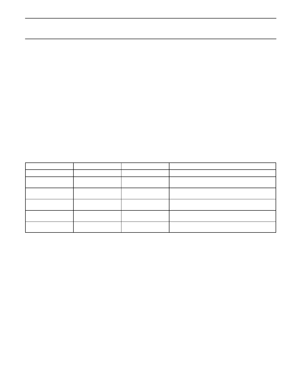
Function Table1
WP
MUX_SELECT_0
MUX_SELECT_1
COMMANDS
0
X
X
Write to the non-volatile registers through I2C bus allowed
1
X
X
Write to the non-volatile registers through I2C bus not
allowed
X
0
1
MUX_OUT and NON_MUXED_OUT (transparent) from
EEPROM byte 0
X
0
0
MUX_OUT and NON_MUXED_OUT (transparent) from
EEPROM byte 1
X
1
1
MUX_OUT from MUX_IN inputs and NON_MUXED_OUT
latched (from EEPROM 0)
X
1
0
NOTE:
1. This table is valid when not overridden by I2C control register.
MUX_OUT from MUX_IN inputs and NON_MUXED_OUT
latched (from EEPROM 1)
POWER-ON RESET (POR)
When power is applied to VDD, an internal power-on reset holds the PCA9560 in a reset state until VDD has reached VPOR. At that point, the
reset condition is released and the PCA9560 volatile registers and I2C/SMBus state machine will initialize to their default states.
The MUX_OUT and NON_MUXED_OUT pin values depend on:
- the MUX_SELECT_0 and MUX_SELECT_1 logic levels, selecting either the MUX_IN input pins or one of the two 6-bit EEPROMs
- the previously stored values in the EEPROM registers/current MUX_IN pin values as shown in the Function Table
2003 Jun 27
6
Share Link: 