PCA9558 Просмотр технического описания (PDF) - Philips Electronics
Номер в каталоге
Компоненты Описание
производитель
PCA9558
Philips Electronics

PCA9558 Datasheet PDF : 18 Pages
| |||
Philips Semiconductors
8-bit I2C and SMBus I/O port with 5-bit multiplexed/1-bit
latched 6-bit I2C EEPROM and 2 k bit EEPROM
Product data
PCA9558
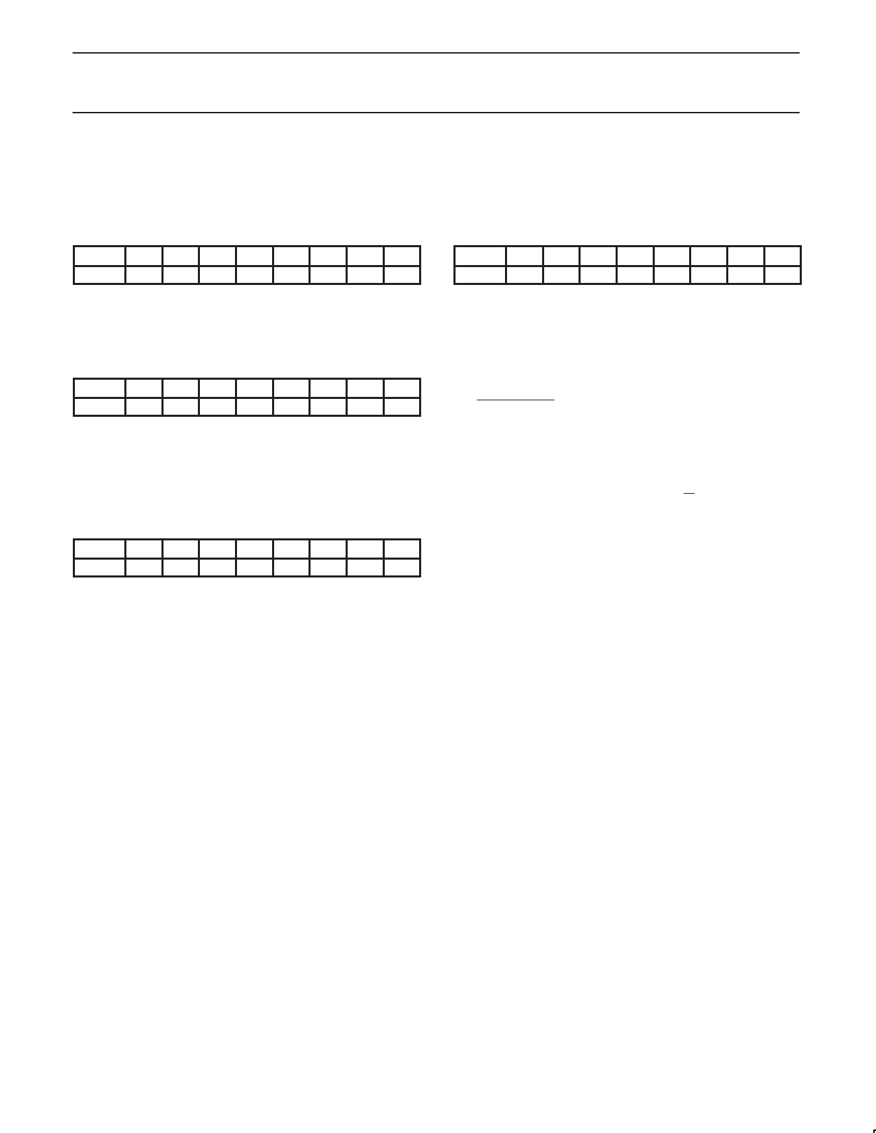
The GPIOs are controlled by a set of 4 internal registers: Input Port Register (IPR); Output Port Register (OPR); Polarity Inversion Register
(PIR); and the Input/Output Configuration Register (IOCR). Each register is read/write via the I2C-bus or 256 byte EEPROM, with the exception
of the IPR, which is read only, one at a time. The read/write takes place on the slave ACKNOWLEDGE. The control of which register is currently
available to the I2C-bus is set by bits in the control register. See Tables 2 through 5 for details.
Table 2. Input Port Register (IPR)
Bit
I7 I6 I5 I4 I3 I2 I1 I0
Default 0
0
0
0
0
0
0
0
Table 5. I/O Configuration Register (IOCR)
Bit C7 C6 C5 C4 C3 C2 C1 C0
Default 0
0
0
0
0
0
0
0
This register is an input-only port. It reflects the logic value present
on the GPIO pins regardless of whether they are configured as
inputs or outputs (IOCR). Writes to this register have no effect.
Table 3. Output Port Register (OPR)
Bit O7 O6 O5 O4 O3 O2 O1 O0
Default 0
0
0
0
0
0
0
0
This register is an output-only port. It reflects the outgoing logic
levels of the GPIO defined as outputs in the IOCR. Bit values in this
register have no effect on GPIO defined as inputs. In turn, reads
from this register reflect the value stored in the flip-flop controlling
the output, not the actual output value.
Table 4. Polarity Inversion Register (PIR)
Bit P7 P6 P5 P4 P3 P2 P1 P0
Default 1
1
1
1
0
0
0
0
This register configures the direction of the GPIO pins. If a bit is set
to a logic 1, the corresponding port pin is enabled as an input with a
high impedance output driver. If a bit is set to a logic 0, the
corresponding port pin is enabled as an output.
Examples of Read/Write to these registers can be found in
Figures 7, 8, 13, and 14.
The I/O_OUT_LOW input, when held LOW longer than the time tW,
will reset the GPIO registers to their default (power-up) values.
A read of the present value of the inputs MUX_INx can be done via
the I2C. This is done by addressing the PCA9558 in a write mode
and entering the correct command code. The preset value on the
MUX_INx inputs is latched at the command code ACKNOWLEDGE.
A REPEATED START is then sent with the R/W bit set to a logic 1,
read, and this latched data is read out on the I2C-bus. See Figure 9.
This register enables polarity inversion of GPIO defined as inputs by
the IOCR. If a bit in this register is set to a logic 1, the corresponding
GPIO input port is inverted. If a bit in this register is set to a logic 0,
the corresponding GPIO input port is not inverted.
2002 May 24
7
Share Link: