PCA9512BD Просмотр технического описания (PDF) - NXP Semiconductors.
Номер в каталоге
Компоненты Описание
производитель
PCA9512BD Datasheet PDF : 27 Pages
| |||
NXP Semiconductors
PCA9512A; PCA9512B
Level shifting hot swappable I2C-bus and SMBus bus buffer
rising edge accelerator (about 0.6 V). With great care a system with four buffers may
work, but as the VOL moves up from 0.1 V, noise or bounces on the line will result in firing
the rising edge accelerator thus introducing false clock edges. Generally it is
recommended to limit the number of buffers in series to two, and to keep the load light to
minimize the offset.
The PCA9510A (rise time accelerator is permanently disabled) and the PCA9512A (rise
time accelerator can be turned off) are a little different with the rise time accelerator turned
off because the rise time accelerator will not pull the node up, but the same logic that turns
on the accelerator turns the pull-down off. If the VIL is above ~0.6 V and a rising edge is
detected, the pull-down will turn off and will not turn back on until a falling edge is
detected.
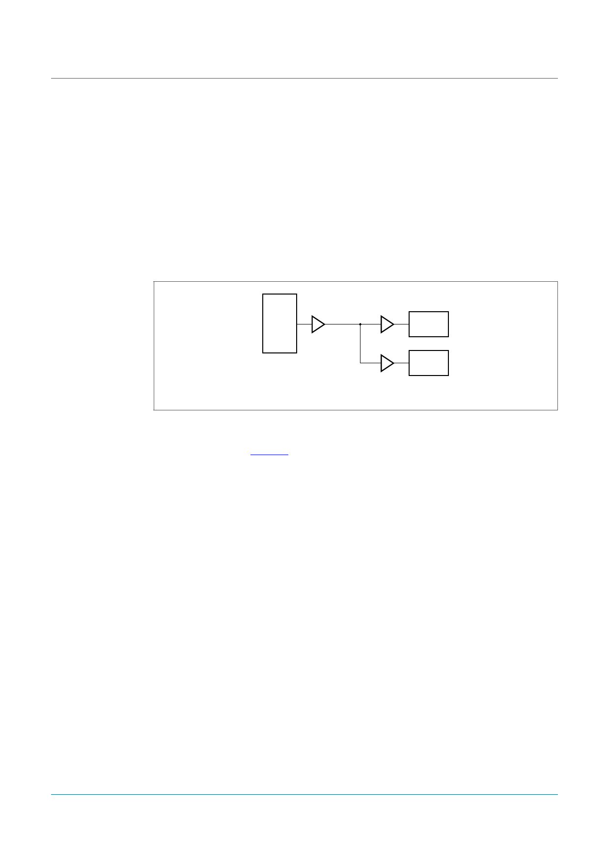
MASTER
buffer A
common
node
buffer B
buffer C
SLAVE B
SLAVE C
002aab581
Fig 4. System with 3 buffers connected to common node
Consider a system with three buffers connected to a common node and communication
between the Master and Slave B that are connected at either end of buffer A and buffer B
in series as shown in Figure 4. Consider if the VOL at the input of buffer A is 0.3 V and the
VOL of Slave B (when acknowledging) is 0.4 V with the direction changing from Master to
Slave B and then from Slave B to Master. Before the direction change you would observe
VIL at the input of buffer A of 0.3 V and its output, the common node, is ~0.4 V. The output
of buffer B and buffer C would be ~0.5 V, but Slave B is driving 0.4 V, so the voltage at
Slave B is 0.4 V. The output of buffer C is ~0.5 V. When the Master pull-down turns off, the
input of buffer A rises and so does its output, the common node, because it is the only part
driving the node. The common node will rise to 0.5 V before buffer B’s output turns on, if
the pull-up is strong the node may bounce. If the bounce goes above the threshold for the
rising edge accelerator ~0.6 V the accelerators on both buffer A and buffer C will fire
contending with the output of buffer B. The node on the input of buffer A will go HIGH as
will the input node of buffer C. After the common node voltage is stable for a while the
rising edge accelerators will turn off and the common node will return to ~0.5 V because
the buffer B is still on. The voltage at both the Master and Slave C nodes would then fall to
~0.6 V until Slave B turned off. This would not cause a failure on the data line as long as
the return to 0.5 V on the common node (~0.6 V at the Master and Slave C) occurred
before the data setup time. If this were the SCL line, the parts on buffer A and buffer C
would see a false clock rather than a stretched clock, which would cause a system error.
PCA9512A_PCA9512B
Product data sheet
All information provided in this document is subject to legal disclaimers.
Rev. 6 — 1 March 2013
© NXP B.V. 2013. All rights reserved.
7 of 27
Share Link: 