PCA9512ADP(2009) Просмотр технического описания (PDF) - NXP Semiconductors.
Номер в каталоге
Компоненты Описание
производитель
PCA9512ADP Datasheet PDF : 23 Pages
| |||
NXP Semiconductors
7. Pinning information
7.1 Pinning
PCA9512A
Level shifting hot swappable I2C-bus and SMBus bus buffer
VCC2 1
8 VCC
SCLOUT 2
7 SDAOUT
PCA9512AD
SCLIN 3
6 SDAIN
GND 4
5 ACC
002aab789
Fig 2. Pin configuration for SO8
VCC2 1
SCLOUT 2
SCLIN 3
GND 4
PCA9512ADP
8 VCC
7 SDAOUT
6 SDAIN
5 ACC
002aab790
Fig 3. Pin configuration for TSSOP8
7.2 Pin description
Table 3. Pin description
Symbol Pin Description
VCC2
1
Supply voltage for devices on the card I2C-bus. Connect pull-up resistors
from SDAOUT and SCLOUT to this pin.
SCLOUT 2
serial clock output to and from the SCL bus on the card
SCLIN
3
serial clock input to and from the SCL bus on the backplane
GND
4
ground supply; connect this pin to a ground plane for best results.
ACC
SDAIN
5
CMOS threshold digital input pin that enables and disables the rise time
accelerators on all four SDAn and SCLn pins. ACC enables all accelerators
when set to VCC2, and turns them off when set to GND.
6
serial data input to and from the SDA bus on the backplane
SDAOUT 7
serial data output to and from the SDA bus on the card
VCC
8
supply voltage; from the backplane, connect pull-up resistors from SDAIN
and SCLIN to this pin.
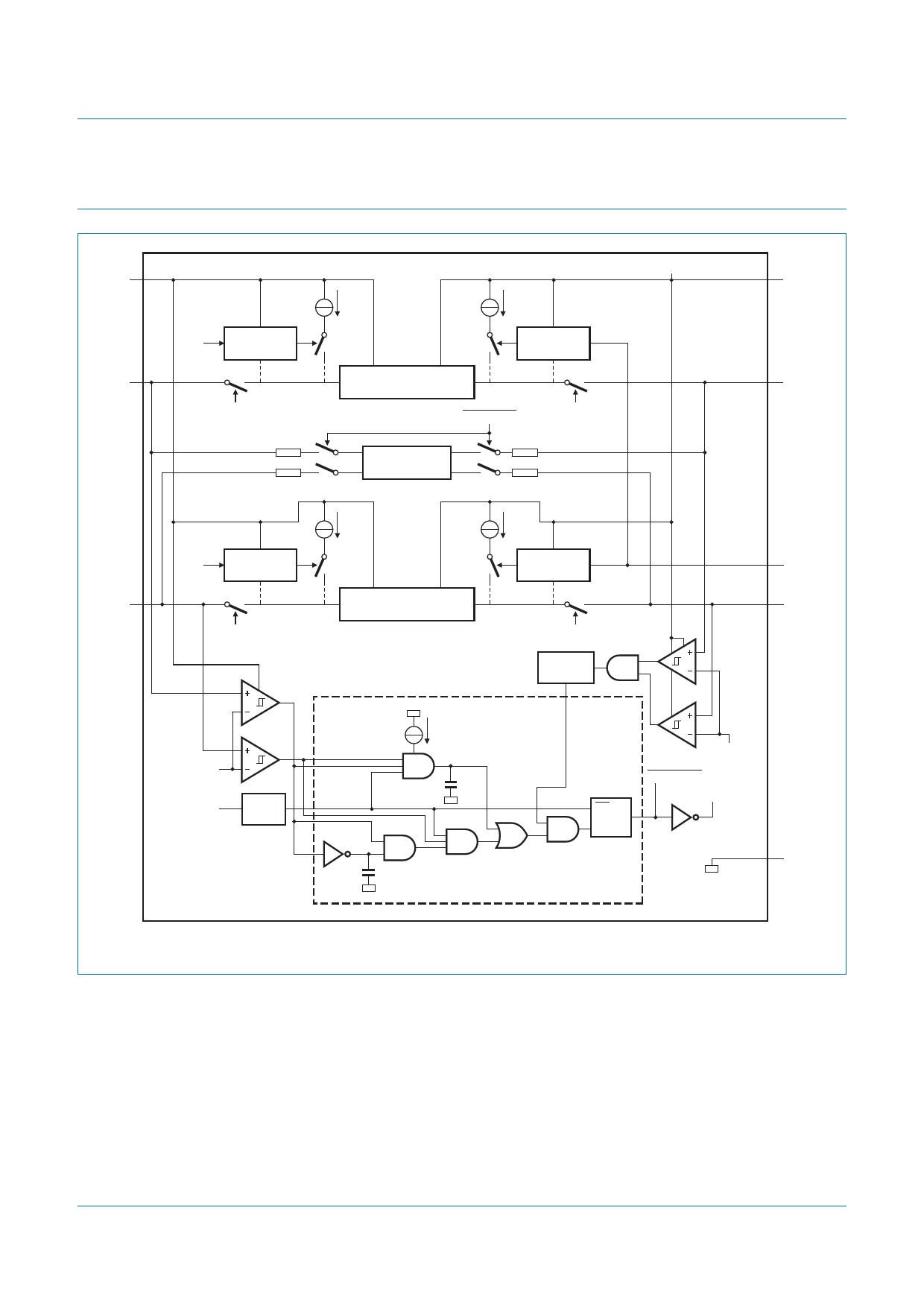
8. Functional description
Refer to Figure 1 “Block diagram of PCA9512A”.
8.1 Start-up
When the PCA9512A is powered up, either VCC or VCC2 may rise first and either may be
more positive or they may be equal, however the PCA9512A will not leave the
undervoltage lock out or initialization state until both VCC and VCC2 have gone above
2.5 V. If either VCC or VCC2 drops below 2.0 V it will return to the undervoltage lock out
state. In the undervoltage lock out state the connection circuitry is disabled, the rise time
accelerators are disabled, and the precharge circuitry is also disabled. After both VCC and
VCC2 are valid, independent of which is higher, the PCA9512A enters the initialization
state; during this state the 1 V precharge circuitry is activated and pulls up the SDAn and
SCLn pins to 1 V through individual 100 kΩ nominal resistors. At the end of the
initialization state the ‘Stop bit and bus idle’ detect circuit is enabled. When all the SDAn
and SCLn pins have been HIGH for the bus idle time or when all pins are HIGH and a
PCA9512A_4
Product data sheet
Rev. 04 — 19 August 2009
© NXP B.V. 2009. All rights reserved.
4 of 23
Share Link: 