PCA5010 Просмотр технического описания (PDF) - Philips Electronics
Номер в каталоге
Компоненты Описание
производитель
PCA5010 Datasheet PDF : 112 Pages
| |||
Philips Semiconductors
Pager baseband controller
Product specification
PCA5010
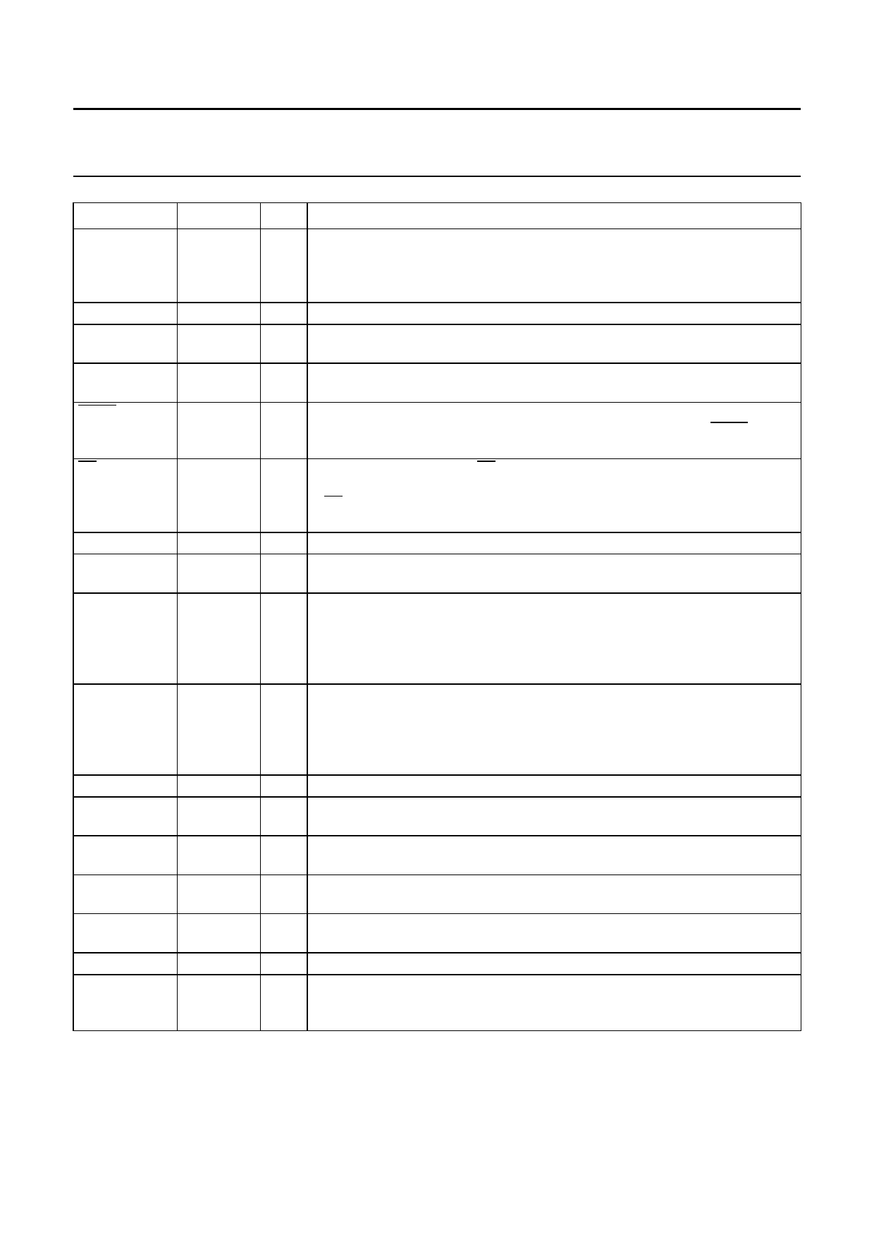
SYMBOL
P1.4
VSS
VDD
ALE
PSEN
EA
TCLK
VPP
P1.6
P1.7
XTL2
XTL1
VBAT
VDD(DC)
VIND
VSS(DC)
RESETIN
PIN TYPE
DESCRIPTION
29
I/O If the UART is disabled (ENS1 in S1CON.4 = 0) then P1.4 can be used as
general purpose P1 port pin. If the UART function is required, then a logic 1
must be written to P1.4. This I/O then becomes the TXD/clock line of the UART.
P1.4 has external interrupt INT6 (X6) assigned.
30
S ground (connected to substrate)
31
S supply voltage for the core logic and most peripheral drivers of the PCA5010
(see VDDA)
32
I/O Address Latch Enable: Output pulse for latching the low byte of the address
during an access to external memory.
33
I/O Program Store Enable: The read strobe to external program memory. When
the device is executing code from the external program memory, PSEN is
activated for each code byte fetch.
34
I/O External Access Enable: EA must be externally held LOW to enable the
device to fetch code from external program memory locations 0000H to 7FFFH.
If EA is held HIGH, the device executes from internal program memory unless
the program counter contains an address greater the 7FFFH (32 kbytes).
35
I clock input for use as timing reference in external access mode and emulation
36
S Programming voltage (12.5 V) for the OTP. Is connected to VSS in the
application.
37
I/O If the I2C-bus is disabled (ENS1 in S1CON.6 = 0) then P1.6 can be used as
general purpose P1 port pin. If the I2C-bus function is required, then a logic 1
must be written to P1.6. This I/O then becomes the clock line of the I2C-bus.
P1.6 is equipped with an open-drain output buffer. The pin has no clamp diode
to VDD.
38
I/O If the I2C-bus is disabled (ENS1 in S1CON.6 = 0) then P1.7 can be used as
general purpose P1 port pin. If the I2C-bus function is required, then a logic 1
must be written to P1.7. This I/O then becomes the data line of the I2C-bus.
P1.7 is equipped with an open-drain output buffer. The pin has no clamp diode
to VDD.
39
O output from the current source oscillator amplifier
40
I input to the inverting oscillator amplifier and time reference for pager decoder,
real-time clock and timers
41
S Supply terminal from battery. Is used for supplying parts of the chip that need to
operate at all times.
42
O Supply voltage output of the DC/DC converter. An external capacitor is
required.
43
I Current input for the DC/DC converter. The booster inductor needs to be
connected externally.
44
S ground (connected to substrate) OTP
45
I Schmitt trigger reset input for the PCA5010. External R and C need to be
connected to the battery supply. All internal storage elements (except
microcontroller RAM) are initialized when this input is activated.
1998 Nov 02
7
Share Link: 