S3C9658 Просмотр технического описания (PDF) - Samsung
Номер в каталоге
Компоненты Описание
производитель
S3C9658 Datasheet PDF : 27 Pages
| |||
PRODUCT OVERVIEW
S3C9654/C9658/P9658
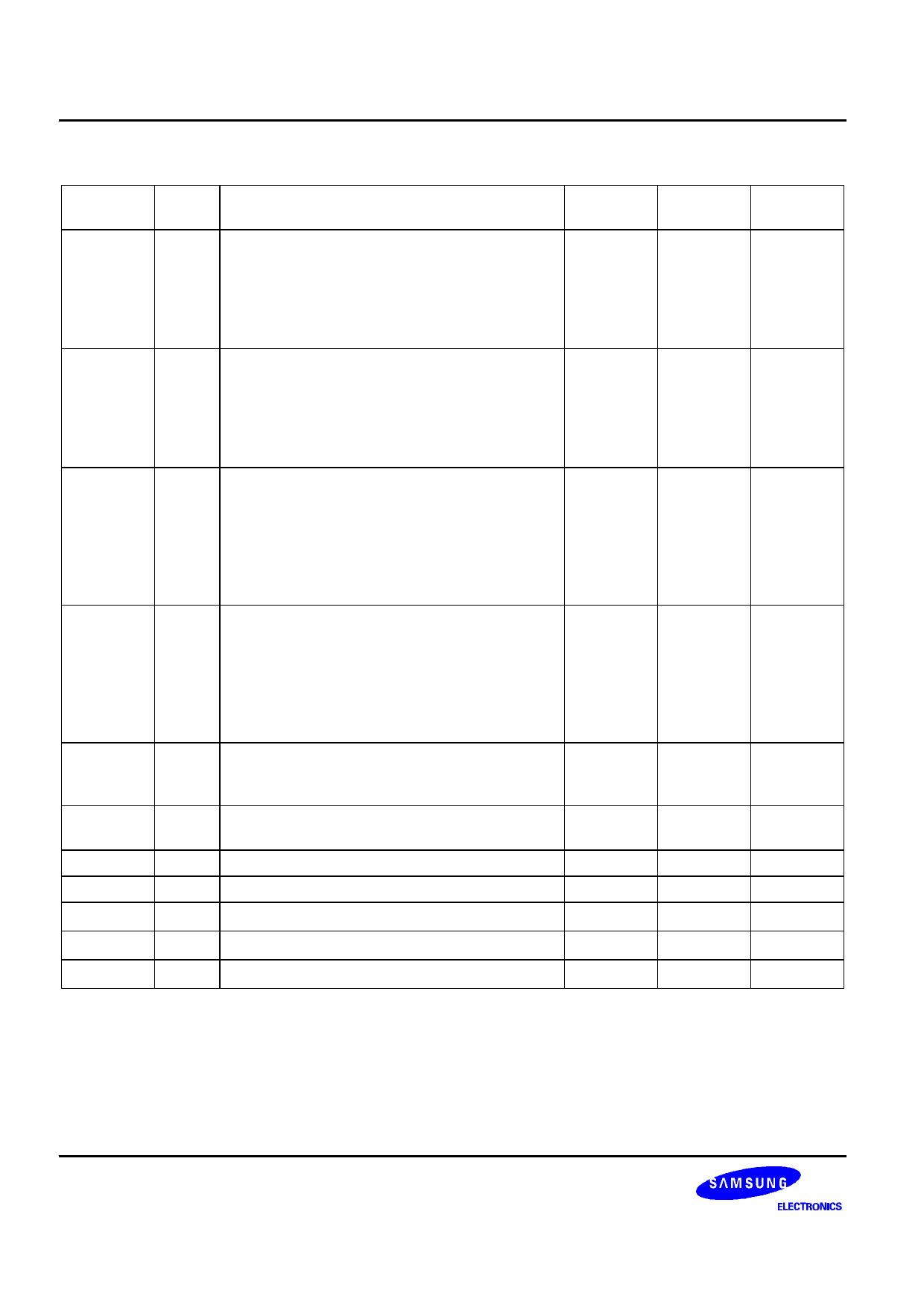
Table 1-1. Signal Descriptions
Pin Names
P0.0
P0.1–P0.5
P1.0–P1.5
P2.0/D-
–
P2.1/D+
XOUT, XIN
INT0
Pin
Type
I/O
I/O
I/O
I/O
–
I
Pin Description
Bit-programmable I/O port for Schmitt trigger
input or n-ch open drain output (50 mA).
Pull-up resistor is assignable to input pin by
software and is automatically disabled for
output pin. Port 0 can be individually configured
as external interrupt input.
Bit-programmable I/O port for Schmitt trigger
input or push-pull output. Pull-up resistors
individually assignable to input pins by software
and are automatically disabled for output pins.
Port 0 can be individually configured as
external interrupt inputs.
Bit-programmable I/O port for Schmitt trigger
input or push-pull output. Pull-up resistors are
individually assignable to input pins by
software. Port 1 can be configured as
comparator input or external interrupt inputs.
Pull-down resistors are individually assignable.
(in comparator input)
Bit-programmable I/O port for Schmitt trigger
input or n-ch open drain output. Pull-up
resistors are individually assignable to input
pins by software and are automatically disabled
for output pins. Port 2 can be individually
configured as external interrupt inputs. Also it
can be configured as an USB ports.
System clock input and output pin
(crystal/ceramic oscillator, or external clock
source)
External interrupt for bit-programmable port 0
Circuit
Number
SK
D
CP
CP
–
D
INT1
I External interrupt for bit-programmable port 1
D
INT2
I External interrupt for bit-programmable port 2
D
VDD
– Power input pin
–
VSS
– VSS is a ground power for CPU core.
–
RESET
1 Reset input pin (Pull-up register embedded)
–
Pin
Numbers
3
1, 10, 11,
12, 20
4–9
17, 18
14, 15
1, 3, 10,
11, 12, 20
4–9
17, 18
19
2
16
Share
Pins
INT0
INT0
CIN0-5
INT1
INT2
–
Port 0
Port 1
Port 2
–
–
–
1-6
Share Link: 