SPX2700AM3-3.3 Просмотр технического описания (PDF) - Signal Processing Technologies
Номер в каталоге
Компоненты Описание
производитель
SPX2700AM3-3.3 Datasheet PDF : 11 Pages
| |||
SPX2700/01/02
ELECTRICAL CHARACTERISTICS at VIN = VO + 5V, IO = 700mA, CO = 22 µF, unless otherwise specified. Limits in
Boldface type apply over the entire operating temperature range. All other specifications are TA = 25°C.
Parameter
Conditions
Typ.
SPX2700/01/02A
SPX2700/01/02
Units
Min
Max Min
Max
Error Comparator
Output Leakage Current
VOH = 30V
0.01
1.00
1.00
µA
2.00
2.00
Output Low Voltage
VIN = 4.5V
150
250
250
mV
IOL = 400µA
400
400
Upper Threshold Voltage
(Note 8)
60
40
40
mV
25
25
Lower Threshold Voltage
(Note 8)
75
95
95
mV
140
140
Hysteresis
(Note 8)
15
mV
Shutdown Input
Input Logic Voltage
Low (Regulator ON)
High (Regulator OFF)
Shutdown Pin Input Current
VS = 2.4V
30
VS = 30V
450
Regulator Output Current In
3
Shutdown
0.7
0.7
V
2.0
2.0
50
90
µA
100
150
600
800
750
1000
10
15
µA
20
25
Note 1: Output or reference voltage temperature coefficients defined as the worst case voltage change divided by the total temperature range.
Note 2: Unless otherwise specified all limits are guaranteed for Tj = 25°C, VIN = 6V, IL = 100µA and CL = 1µF. Additional conditions for the 8-pin versions are
feedback tied to 5V tap and output tied to output sense (VOUT = 5V) and VSHUTDOWN ≤ 0.8V.
Note 3: Regulation is measured at constant junction temperature, using pulse testing with a low duty cycle. Changes in output voltage due to heating effects are
covered under the specification for thermal regulation.
Note 4: Line regulation for the SPX2700/01/02 is tested at 150°C for IL = 1 mA. For IL = 100µA and TJ = 125°C, line regulation is guaranteed by design to 0.2%. See
typical performance characteristics for line regulation versus temperature and load current.
Note 5: Dropout voltage is defined as the input to output differential at which the output voltage drops 100 mV below its nominal value measured at 1V differential at
very low values of programmed output voltage, the minimum input supply voltage of 2V ( 2.3V over temperature) must be taken into account.
Note 6: VREF ≤VOUT ≤ (Vin - 1V), 2.3 ≤Vin≤30V, 100µA≤IL≤ 250 mA, TJ ≤ TJMAX.
Note 7: Comparator thresholds are expressed in terms of a voltage differential at the feedback terminal below the nominal reference voltage measured at 6V input. To
express these thresholds in terms of output voltage change, multiply by the error amplifier gain = VOUT/VREF = (R1 + R2)/R2. For example, at a programmed output
voltage of 5V, the Error output is guaranteed to go low when the output drops by 95 mV x 5V/1.235 = 384 mV. Thresholds remain constant as a percent of VOUT as
VOUT is varied, with the dropout warning occurring at typically 5% below nominal, 7.5% guaranteed.
Note 8: VSHUTDOWN ≥ 2V, VIN ≤ 30V, VOUT =0, Feedback pin tied to 5V Tap.
Note 9: The junction -to-ambient thermal resistance of the TO-92 package is 180°C/ W with 0.4” leads and 160°C/ W with 0.25” leads to a PC board.
The thermal resistance of the 8-Pin DIP package is 105°C/W junction-to-ambient when soldered directly to a PC board. Junction-to-ambient thermal resistance for the
SOIC (S) package is 160°C/W.
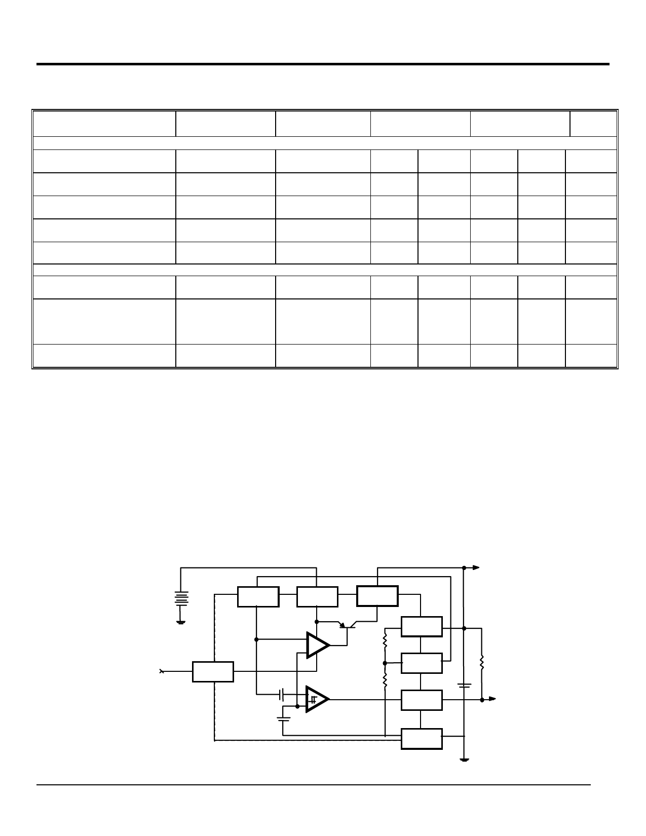
UNREGULATED DC
+
FEEDBACK
INPUT
OUTPUT
5V @ 700mA
MAX
FROM
CMOS OR
TTL
SHUTDOWN
+
_ ERROR
AMPLIFIER
180kΩ ..
+
+
60 mV
_
+ 1.23V
60kΩ ..
ERROR DETECTION
COMPARATOR
REFERENCE
SPX2700/01/02 Block Diagram
SENSE
5V TAP
______
ERROR
GROUND
330kΩ ..
+
1µF..
TO CMOS OR
TTL
Rev. 10/25/00
Share Link: 