AD8184 Просмотр технического описания (PDF) - Analog Devices
Номер в каталоге
Компоненты Описание
производитель
AD8184 Datasheet PDF : 12 Pages
| |||
AD8184
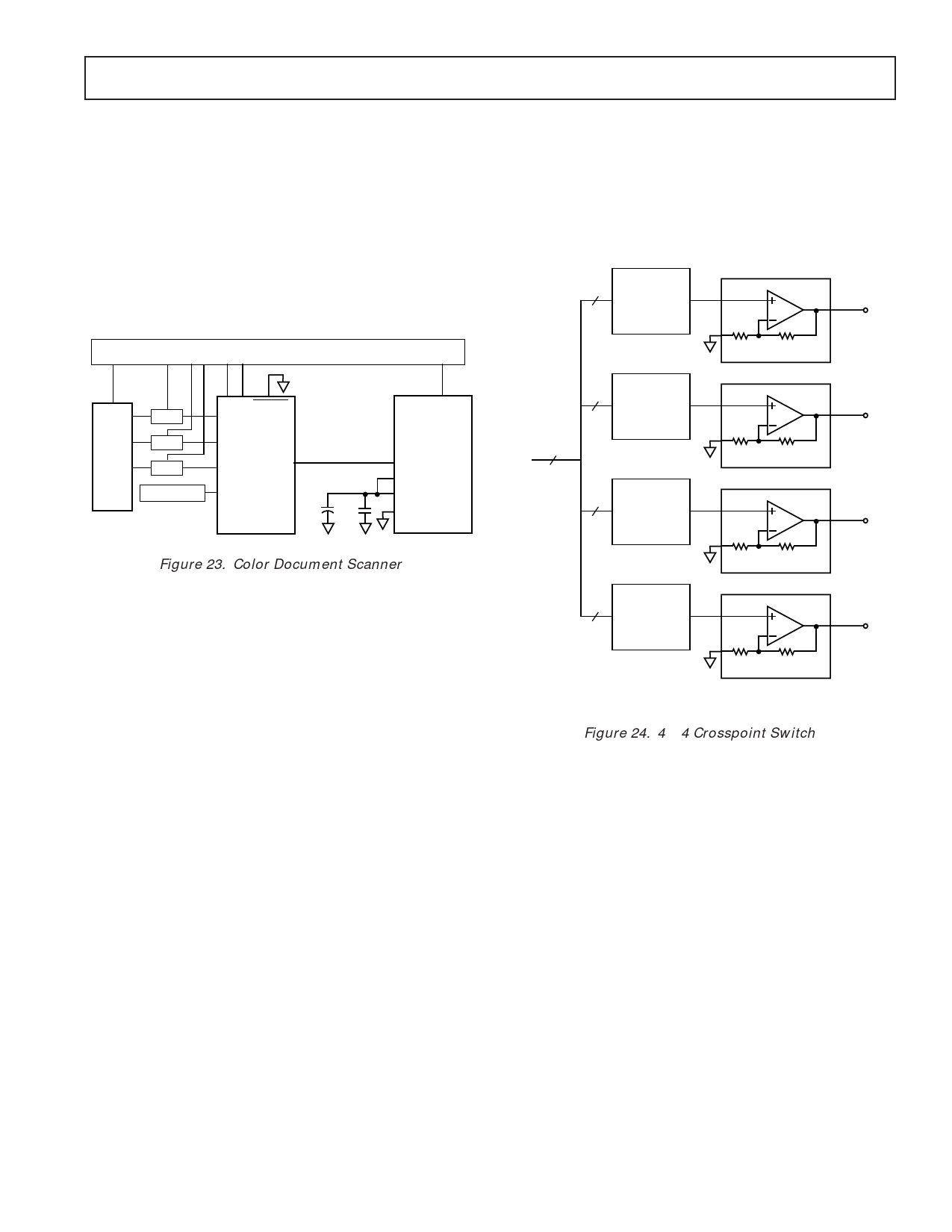
Color Document Scanner
Figure 23 shows a block diagram of a Color Document Scanner.
Charge Coupled Devices (CCDs) find widespread use in scan-
ner applications. A monochrome CCD delivers a serial stream
of voltages levels, each level being proportional to the light shin-
ing on that cell. In the case of the color image scanner shown,
there are three output streams, representing red, green and blue.
Interlaced with the stream of voltage levels is a voltage repre-
senting the reset level (or black level) of each cell. A Correlated
Double Sampler (CDS) subtracts these two voltages from each
other in order to eliminate the relatively large offsets common
with CCDs.
A 4 ؋ 4 Crosspoint Switch
While large crosspoint arrays are best constructed using highly
integrated devices such as the AD8116, 16 × 16 crosspoint
switch, smaller or irregular sized arrays can be constructed using
4-to-1 multiplexers such as the AD8184. The circuit below
shows a 4 × 4 array, constructed using the AD8184 and buff-
ered using the AD8079, a dual, fixed gain of 2 or 2.2, video
amplifier.
AD8184
4
IN0-IN3 OUT
1/2 AD8079*
OUT0
CONTROL & TIMING
750Ω
750Ω
R
G
CCD
B
CDS
CDS
CDS
REFERENCE
A0 A1 ENABLE
OUT
AD8184
10µF
0.1µF
AD9220
10/12-BIT
10MSPS
A/D
CONVERTER
VINA
VINB
VREF
SENSE
AD8184
4
IN0-IN3 OUT
4
IN0-3
AD8184
4
IN0-IN3 OUT
1/2 AD8079*
750Ω
750Ω
OUT1
1/2 AD8079*
OUT2
Figure 23. Color Document Scanner
The next step in the data acquisition process involves digitizing
the three signal streams. Assuming that the analog-to-digital
converter chosen has a fast enough sample rate, multiplexing
the three streams into a single ADC is generally more economi-
cal than using one ADC per channel. In the example shown, we
use the AD8184 as the multiplexer.
Because of its high bandwidth, the AD8184 is capable of driving
the switched capacitor input stage of the AD9220 without addi-
tional buffering. In addition to having the required bandwidth,
it is necessary to consider the settling time of the multiplexer. In
this case, the ADC has a sample rate of 10 MHz, which corre-
sponds to a sampling period of 100 ns. Typically, one phase of
the sampling clock is used for conversion (i.e., all levels are held
steady) and the other is used for switching and settling to the
next channel. Assuming a 50% duty cycle, the signal chain must
settle within 50 ns. With a settling time to 0.1% of 15 ns, the
multiplexer easily satisfies this criterion.
In the example shown, the fourth (spare) channel of the
AD8184 is used to measure a reference voltage. This voltage
would probably be measured less frequently than the R, G and
B signals. Multiplexing a reference voltage offers the advantage
that any temperature drift effects caused by the multiplexer will
equally impact the reference voltage and the to-be-measured sig-
nals. If the fourth channel is unused, it is good design practice
to permanently tie it to ground.
750Ω
750Ω
AD8184
4
IN0-IN3
OUT
1/2 AD8079*
750Ω
750Ω
OUT3
*AD8079 IS A DUAL, FIXED GAIN OF 2 AMPLIFIER
Figure 24. 4 × 4 Crosspoint Switch
REV. 0
–9–
Share Link: 