W91630 Просмотр технического описания (PDF) - Winbond
Номер в каталоге
Компоненты Описание
производитель
W91630 Datasheet PDF : 14 Pages
| |||
W91630 SERIES
Pin Description, continued
SYMBOL PIN NO. I/O
FUNCTION
HKS
DP /C5
DTMF
10
I Hook switch input. Conventional CMOS input with an internal
protection diode and a pull-high resistor to VDD.
HKS = VDD: On-hook state. Chip in sleep mode, no operation.
HKS = VSS: Off-hook state. Chip enabled for normal operation.
During dialing, this input ignores HKS = VDD for durations of less
than 150 mS (i.e., dialing is not terminated).
11
O Open drain dialing pulse output (Figure 1).
Flash key causes DP /C5 to be active in both tone mode and pulse
mode.
12
O During pulse dialing, maintains low state at all times.
In tone mode, outputs a dual or single tone.
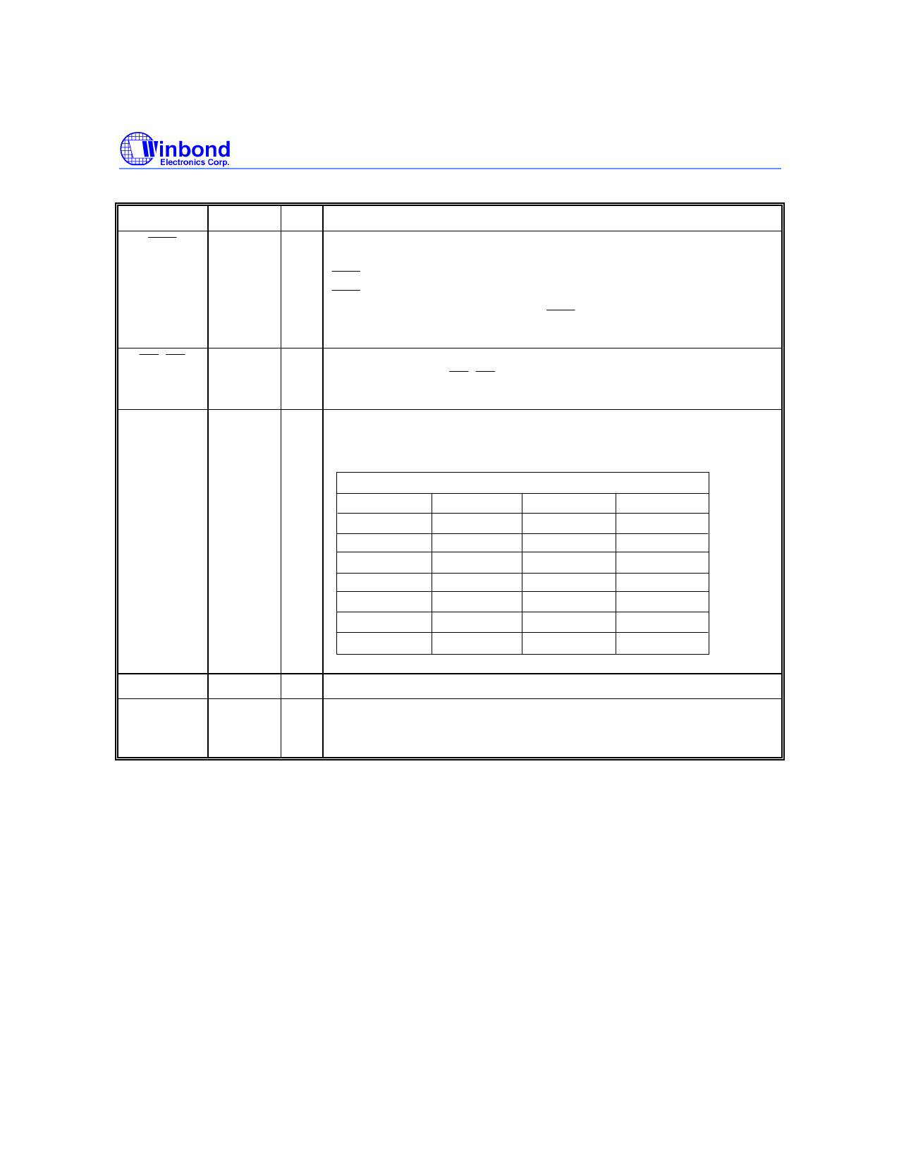
Detailed timing diagram for tone mode is shown in Figure 2(a, b).
OUTPUT FREQUENCY
Specified
Actual
Error %
R1
697
699
+0.28
R2
770
766
-0.52
R3
852
848
-0.47
R4
941
948
+0.74
C1
1209
1216
+0.57
C2
1336
1332
-0.30
C3
1477
1472
-0.34
VDD, VSS
P MUTE
14, 6
5
I Power input pins.
O The P MUTE is a conventional CMOS inverter output. It is high
during pulse dialing sequence and flash break. Otherwise, it
remains low.
Publication Release Date: June 1996
-3-
Revision A3
Share Link: 