OM6211 –ü—Ä–æ—Å–º–æ—Ç—Ä —Ç–µ—Ö–Ω–∏—á–µ—Å–∫–æ–≥–æ –æ–ø–∏—Å–∞–Ω–∏—è (PDF) - Philips Electronics
–ù–æ–º–µ—Ä –≤ –∫–∞—Ç–∞–ª–æ–≥–µ
–ö–æ–º–ø–æ–Ω–µ–Ω—Ç—ã –û–ø–∏—Å–∞–Ω–∏–µ
–ø—Ä–æ–∏–∑–≤–æ–¥–∏—Ç–µ–ª—å
OM6211 Datasheet PDF : 48 Pages
| |||
Philips Semiconductors
48 √ó 84 dot matrix LCD driver
Product specification
OM6211
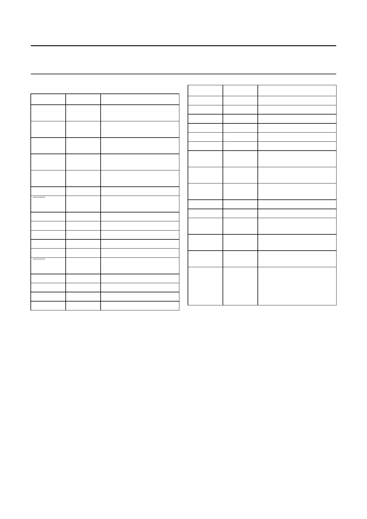
6 PINNING
SYMBOL
VOS4
PAD
3
VOS3
4
VOS2
5
VOS1
6
VOS0
7
T6
RES
8 to 11
16
T5
17
T4
18
T3
19
T2
20
T1
21
SCE
22
VSS2
VSS1
OSC
SDOUT
23 to 30
31 to 38
40
41
DESCRIPTION
input pin 4 for VLCD
calibration
input pin 3 for VLCD
calibration
input pin 2 for VLCD
calibration
input pin 1 for VLCD
calibration
input pin 0 for VLCD
calibration
test input 6
external reset input
(active LOW)
test input 5
test input 4
test output 3
test output 2
test output 1
chip enable input
(active LOW)
ground
ground
oscillator input
serial data output
SYMBOL
SDIN
SCLK
ID4
ID3
MX
VDD1
VDD2
VDD3
VLCDSENSE
VLCDOUT
VLCDIN
ROW 0 to
ROW 23
COL 0 to
COL 83
ROW 47 to
ROW 24
PAD
42
43
44
45
46
47 to 52
53 to 60
61 to 64
65
66 to 72
73 to 78
89 to 112
DESCRIPTION
serial data input
serial clock input
module identification input
module identification input
horizontal mirroring input
logic supply voltage
voltage multiplier supply
voltage
voltage multiplier supply
voltage
VLCD generator regulation
input
VLCD generator output
LCD supply voltage input
LCD row driver outputs
113 to 196 LCD column driver outputs
197 to 220 LCD row driver outputs
1, 12 to 15,
39, 79,
81 to 88
and
221 to 225
dummy pads
7 PIN FUNCTIONS
7.1 ROW 0 to ROW 47 row driver outputs
These pads output the display row signals.
7.2 COL 0 to COL 83 column driver outputs
These pads output the display column signals.
7.3 VSS1 and VSS2: negative power supply rails
Negative power supply rails VSS1 and VSS2 must be
connected together, hereafter referred to as VSS. When a
pin has to be connected externally to VSS, then pin VSS1
should be used.
7.4 VDD1 to VDD3: positive power supply rails
Positive power supply rails: VDD1 for logic supply, VDD2 and
VDD3 for voltage multiplier. VDD2 and VDD3 must be
connected together, hereafter referred to as VDD2.
7.5 VLCDOUT, VLCDIN and VLCDSENSE: LCD power
supply
If the internal VLCD generator is used, then all three pins
must be connected together. If not (VLCD generator is
disabled and an external voltage is applied to VLCDIN), then
VLCDOUT must be left open-circuit, VLCDSENSE must be
connected to VLCDIN, VDD2 and VDD3 should be applied
according to the specified voltage range. The following
settings are also required: HVE = 0, S1 = 1 and S0 = 0.
7.6 VOS4 to VOS0: calibration inputs
Five pull-up input pins for on-glass VLCD calibration. Each
pin may be connected to VSS, which corresponds to
logic 0, or left open-circuit, which corresponds to logic 1.
All five pins define a 5-bit two’s complement number
ranging from ‚àí16 to 15 decimal (from 10000 to 01111).
The default value, with all pins connected to VSS, is
0 decimal (00000).
2002 Jan 17
5
Share Link: 