NX2415 Просмотр технического описания (PDF) - Microsemi Corporation
Номер в каталоге
Компоненты Описание
производитель
NX2415
Microsemi Corporation

NX2415 Datasheet PDF : 21 Pages
| |||
NX2415
Control Loop Compensator Design
NX2415 can control and drive two channel synchro-
nous bucks with 180o phase shift between each other.
One of two channels is called master, the other is called
slave. They are connected together by sharing the same
output capacitors. Voltage loop is designed to regulate
output voltage. In order to achieve the current balance in
these two synchronous buck converters, current loop
compensation network is employed to to make sure the
currents in slave is following the master.
Voltage Loop Compensator Design
Due to the double pole generated by LC filter of the
power stage, the power system has 180o phase shift ,
and therefore, is unstable by itself. In order to achieve
accurate output voltage and fast transient
response,compensator is employed to provide highest
possible bandwidth and enough phase margin. Ideally,
the Bode plot of the closed loop system has crossover
frequency between 1/10 and 1/5 of the switching fre-
quency, phase margin greater than 50o and the gain cross-
ing 0dB with -20dB/decade. Power stage output capaci-
tors usually decide the compensator type. If electro-
lytic capacitors are chosen as output capacitors, type II
compensator can be used to compensate the system,
because the zero caused by output capacitor ESR is
lower than crossover frequency. Otherwise type III com-
pensator should be chosen.
A. Type III compensator design
For low ESR output capacitors, typically such as
Sanyo OSCON and POSCAP, the frequency of ESR zero
caused by output capacitors is higher than the cross-
over frequency. In this case, it is necessary to compen-
sate the system with type III compensator.
In design example, six electrolytic capacitors are
used as output capacitors. The system is compensated
with type III compensator. The following figures and equa-
tions show how to realize the this type III compensator
with electrolytic capacitors.
FZ1
=
2×
π
1
× R4
×
C2
FZ2
=
1
2 × π × (R2 + R3 ) × C3
FP1
=
2×
π
1
× R3
×
C3
FP2
=
1
2
×
π
×
R4
×
C1
C1
×
+
C2
C2
...(11)
...(12)
...(13)
...(14)
where FZ1,FZ2,FP1 and FP2 are poles and zeros in
the compensator.
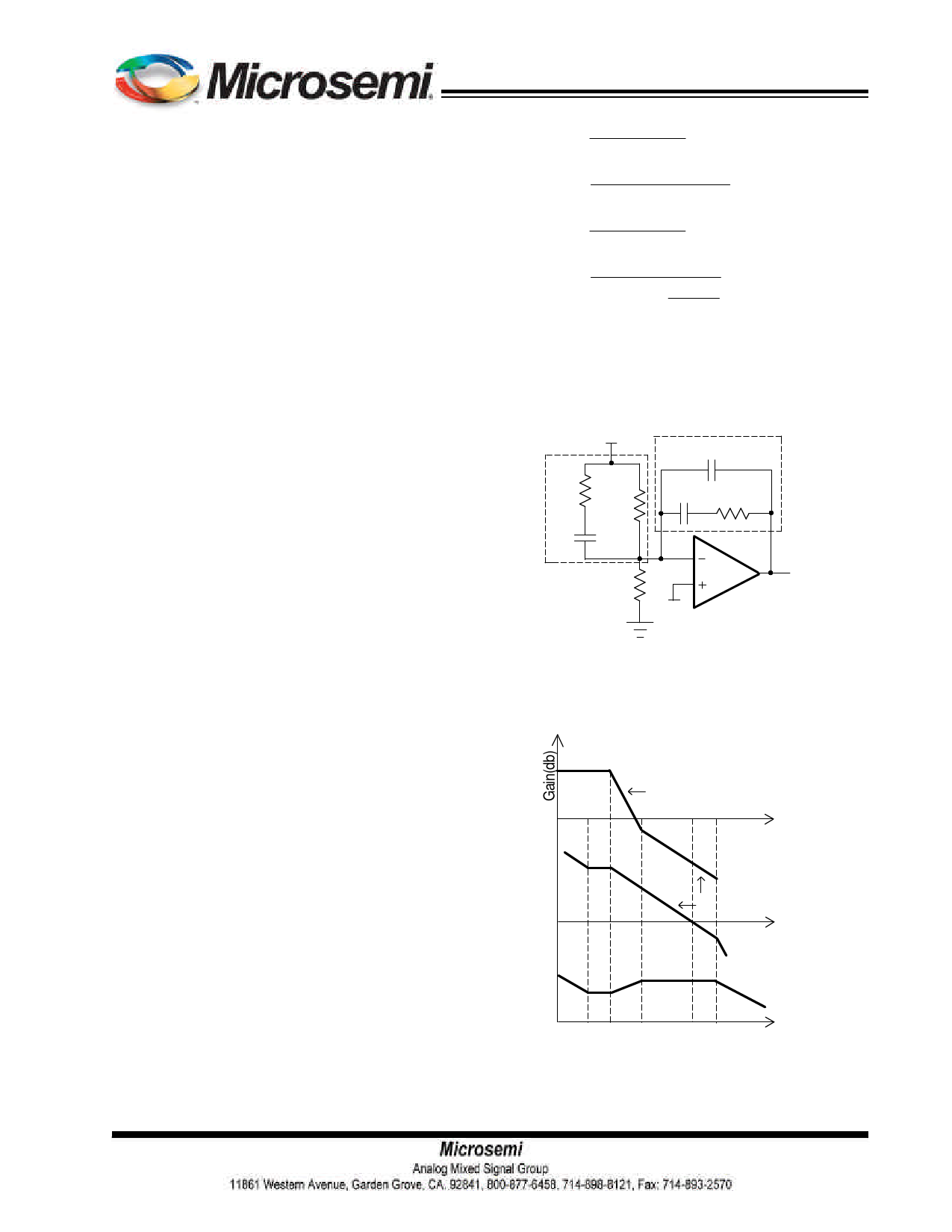
Vout
Zf
Zin
C1
R3
R2
C2 R4
C3
Fb
Ve
R1
Vref
Figure 2 - Type III compensator
power stage
FLC
40dB/decade
loop gain
F ESR
compensator
20dB/decade
FZ1 FZ2 FP1
FO FP2
Rev.4.8
05/06/08
Figure 3 - Bode plot of Type III compensator
10
Share Link: