NTE922M Просмотр технического описания (PDF) - NTE Electronics
Номер в каталоге
Компоненты Описание
производитель
NTE922M Datasheet PDF : 4 Pages
| |||
Absolute Maximum Ratings (Cont’d):
Output Short Circuit Duration . . . . . . . . . . . . . . . . . . . . . . . . . . . . . . . . . . . . . . . . . . . . . . . . . . . . . . 10sec
Operating Temperature Range . . . . . . . . . . . . . . . . . . . . . . . . . . . . . . . . . . . . . . . . . . . . . . . 0° to +70°C
Storage Temperature Range . . . . . . . . . . . . . . . . . . . . . . . . . . . . . . . . . . . . . . . . . . . . . . –65° to +150°C
Lead Temperature (During Soldering, 10 sec) . . . . . . . . . . . . . . . . . . . . . . . . . . . . . . . . . . . . . . +260°C
Voltage at Strobe Pin . . . . . . . . . . . . . . . . . . . . . . . . . . . . . . . . . . . . . . . . . . . . . . . . . . . . . . . . . . . . V+ –5V
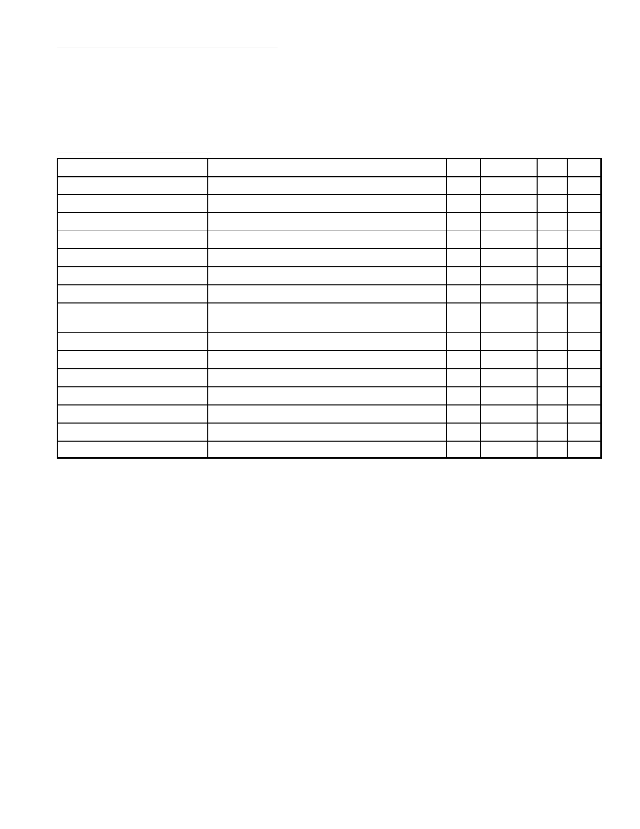
Electrical Characteristics: (Note 3)
Parameter
Test Conditions
Input Offset Voltage
Input Offset Current
Input Bias Current
Voltage Gain
Response Time
Saturation Voltage
Strobe ON Current
Output Leakage Current
Input Offset Voltage
Input Offset Current
TA = +25°C, RS ≤ 50k, Note 4
TA = +25°C, Note 4
TA = +25°C
TA = +25°C
TA = +25°C, Note 5
VIN ≤ –10mV, IOUT = 50mA, TA = +25°C
TA = +25°C
VIN ≥ 10mV, VOUT = 35V TA = +25°C,
ISTROBE = 3mA, V– = VGRND = –5V
RS ≤ 50K, Note 4
Note 4
Input Bias Current
Input Voltage Range
Saturation Voltage
Positive Supply Current
Negative Supply Current
V+ ≥ 4.5V, V– = 0, VIN ≤ –10mV, ISINK ≤ 8mA
TA = +25°C
TA = +25°C
Min
Typ Max Unit
–
2.0
7.5 mV
–
6.0
50 nA
–
100 250 nA
40
200
– V/mV
–
200
– ns
–
0.75 1.5 V
1.5
3.0
– mA
–
0.2
59 nA
–
–
10 mV
–
–
70 nA
–
–
300 nA
–14.5 13.8,–14.7 13.0 V
–
0.23 0.4 V
–
5.1
7.5 mA
–
4.1
5.0 mA
Note 3. These specifications apply for VS = ±15V and the Ground pin at GND, and 0°C < TA < +70°C,
unless otherwise specified. The offset voltage, offset current and bias current specifications
apply for any supply voltage from a single 5V supply up to ± 15V supplies.
Note 4. The offset voltages and offset currents given are the maximum values required to drive the
output within a volt of either supply with 1mA load. Thus, these parameters define an error
band and take into account the worst–case effects of voltage gain and input impedance.
Note 5. Do not short the strobe pin to ground: it should be current driven at 3 to 5mA.
Share Link: 