NTE7114 Просмотр технического описания (PDF) - NTE Electronics
Номер в каталоге
Компоненты Описание
производитель
NTE7114 Datasheet PDF : 4 Pages
| |||
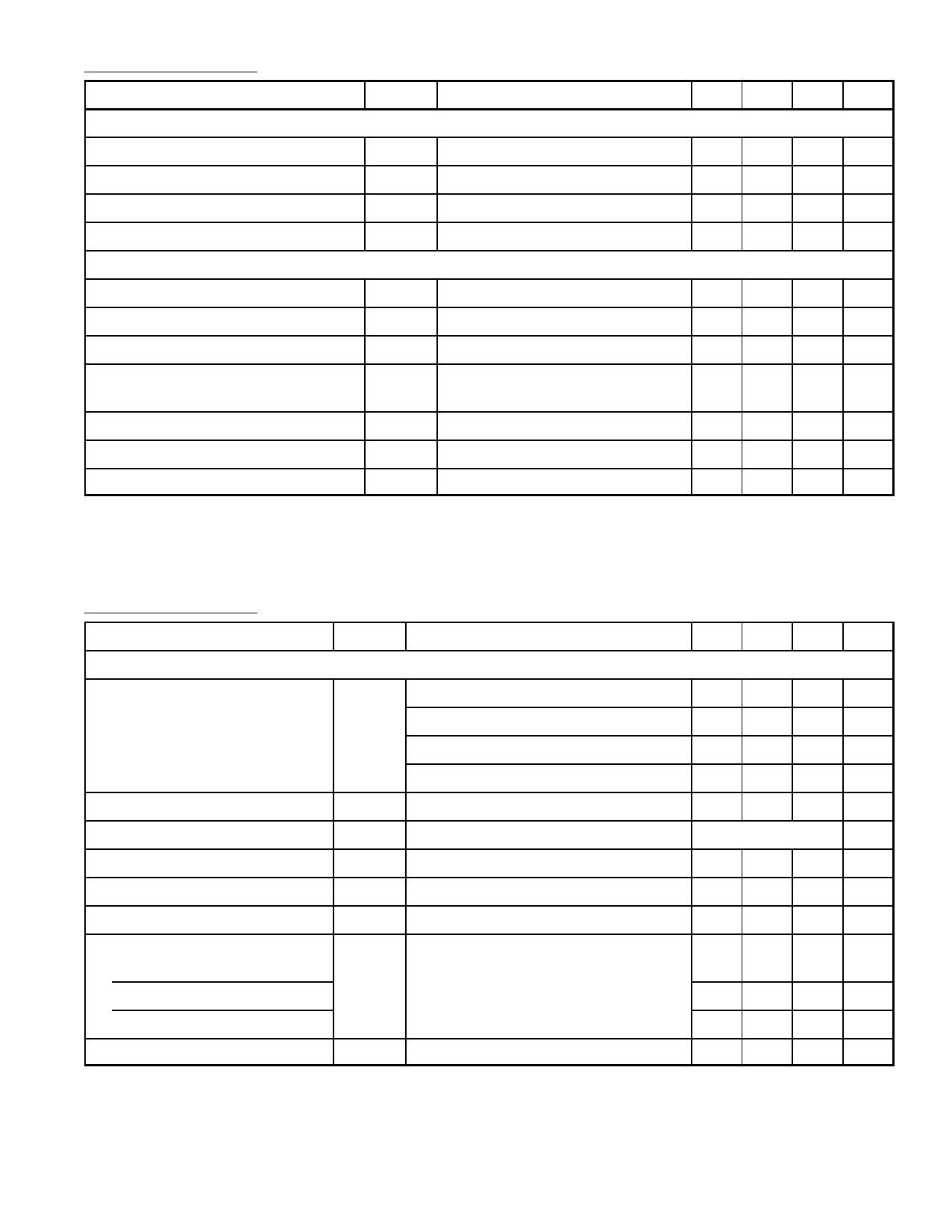
DC Characteristics: (VP = 14.4V, TA = +25°C unless otherwise specified)
Parameter
Symbol
Test Conditions
Min Typ Max Unit
Supply
Supply Voltage Range
Total Quiescent Current
DC Output Voltage
DC Output Offset Voltage
Mute/Stand−by Switch
VP
Itot
VO
|∆VO|
Note 1
Note 2
8.0 14.4 18.0 V
− 80 180 mA
− 8.9 − V
− − 100 nV
Switch−ON Voltage Level
Mute Condition
Output Signal in Mute Position
DC Output Offset Voltage
(Between Pins 6 to 8 & 10 to 12)
VON
Vmute
VO
|∆VO|
VI = 1V (max), f = 1kHz
8.5 − − V
3.3 − 6.4 V
− − 2 mV
− − 100 mV
Stand−by Condition
Vsb
DC Current in Stand−by Condition Isb
Switch−ON Current
Isw
0−2V
− − 100 µA
− 12 40 µA
Note 1. The circuit is DC adjusted at VP = 6V to 18V and AC operating at VP = 8.5V to 18V.
Note 2. At 18V < VP < 30V the DC output voltage ≤ VP/2.
AC Characteristics: (VP = 14.4V, RL = 4Ω, f = 1kHz, TA = +25°C unless otherwise specified)
Parameter
Symbol
Test Conditions
Min Typ Max Unit
Stereo BTL Application
Output Power
PO THD = 0.5%
THD = 0.5%, VP = 13.2V
THD = 10%
15 17 − W
− 12 − W
20 22 − W
THD = 10%, VP = 13.2V
− 17 − W
Total Harmonic Distortion
THD PO = 1W
− 0.1 − %
Power Bandwidth
BW THD = 0.5%, PO = −1dB, w.r.t = 15W
20 to 15000
Hz
Low Frequency Roll−Off
fL −1dB, Note 3
− 45 − Hz
High Frequency Roll−Off
fH −1dB, Note 3
20 − − kHz
Closed Loop Voltage Gain
GV
25 26 27 dB
Supply Voltage Ripple Rejection RR Note 4
ON
48 − − dB
Mute
48 − − dB
Stand−by
80 − − dB
Input Impedence
|Zi|
25 30 38 kΩ
Note 3. Frequency response externally fixed.
Note 4. Ripple Rejection measured at the output with source impedence of 0Ω (maximum ripple
amplitude of 2V) and a frequency between 100Hz and 20kHz.
Share Link: 