NM27C020 Просмотр технического описания (PDF) - Fairchild Semiconductor
Номер в каталоге
Компоненты Описание
производитель
NM27C020 Datasheet PDF : 14 Pages
| |||
Functional Description
DEVICE OPERATION
The six modes of operation of the device are listed in Table 1. It
should be noted that all inputs for the six modes are at TTL levels.
The power supplies required are VCC and VPP. The VPP power
supply must be at 12.75V during the three programming modes,
and must be at 5V in the other three modes. The VCC power supply
must be at 6.5V during the three programming modes, and at 5V
in the other three modes.
Read Mode
The part has two control functions, both of which must be logically
active in order to obtain data at the outputs. Chip Enable (CE) is
the power control and should be used for device selection. Output
Enable (OE) is the output control and should be used to gate data
to the output pins, independent of device selection. Assuming that
the addresses are stable, address access time (tACC) is equal to
the delay from CE to output (tCE). Data is available at the outputs
tOE after the falling edge of OE, assuming that CE has been low
and addresses have been stable for at least tACC –tOE.
Standby Mode
The EPROM has a standby mode which reduces the active power
dissipation by over 99%, from 220 mW to 0.55 mW. The EPROM
is placed in the standby mode by applying a CMOS high signal to
the CE input. When in standby mode, the outputs are in a high
impedance state, independent of the OE input.
Output OR-Tying
Because the part is usually used in larger memory arrays, Fair-
child has provided a 2-line control function that accommodates
this use of multiple memory connections. The 2-line control
function allows for:
1. the lowest possible memory power dissipation, and
2. complete assurance that output bus contention will not
occur.
To most efficiently use these two control lines, it is recommended
that CE be decoded and used as the primary device selecting
function, while OE be made a common connection to all devices
in the array and connected to the READ line from the system
control bus. This assures that all selected memory devices are in
their low power standby modes and that the output pins are active
only when data is desired from a particular memory device.
Programming
CAUTION: Exceeding 14V on pin 1 (VPP) will damage the device.
Initially, and after each erasure, all bits of the device are in the “1’s”
state. Data is introduced by selectively programming “0’s” into the
desired bit locations. Although only “0’s” will be programmed, both
“1’s” and “0’s” can be presented in the data word. The only way to
change a “0” to a “1” is by ultraviolet light erasure.
The part is in the programming mode when the VPP power supply
is at 12.75V and OE is at VIH. It is required that at least a 0.1 µF
capacitor be placed across VPP, VCC to ground to suppress
spurious voltage transients which may damage the device. The
data to be programmed is applied 8 bits in parallel to the data
output pins. The levels required for the address and data inputs
are TTL.
When the address and data are stable, an active low, TTL program
pulse is applied to the PGM input. A program pulse must be
applied at each address location to be programmed. The EPROM
is programmed with the Turbo Programming Algorithm shown in
Figure 1. Each Address is programmed with a series of 50 µs
pulses until it verifies good, up to a maximum of 10 pulses. Most
memory cells will program with a single 50 µs pulse. (The standard
National Semiconductor Algorithm may also be used but it will
have longer programming time.) The EPROM must not be pro-
grammed with a DC signal applied to the PGM input. Program-
ming multiple EPROM in parallel with the same data can be easily
accomplished due to the simplicity of the programming require-
ments. Like inputs of the parallel EPROM may be connected
together when they are programmed with the same data. A low
level TTL pulse applied to the PGM input programs the paralleled
EPROM.
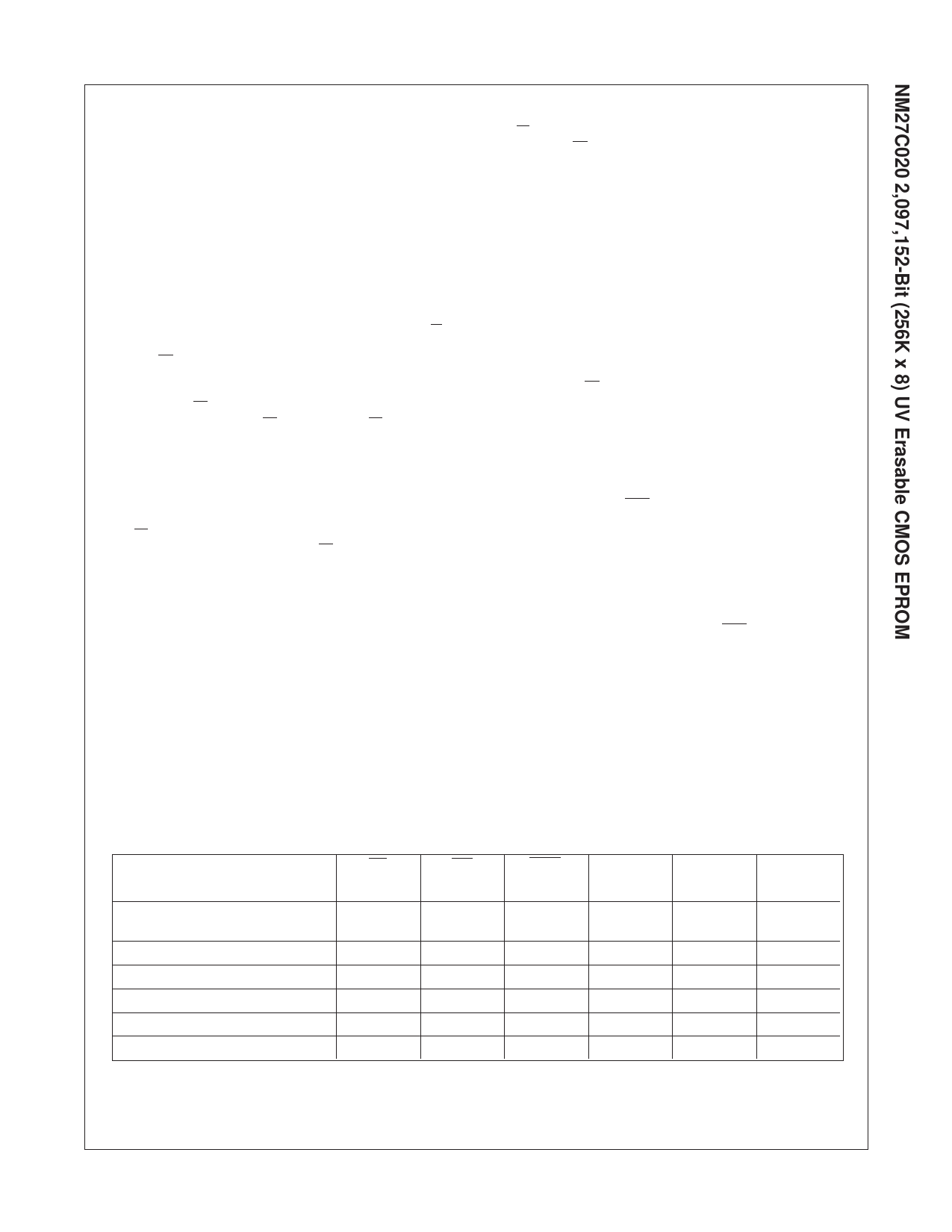
MODE SELECTION
The modes of operation of the NM27C020 are listed in Table 1. A single 5V power supply is required in the read mode. All inputs are
TTL levels except for VPP and A9 for device signature.
TABLE 1. Modes Selection
Mode
Pins
CE
OE
PGM
VPP
VCC
Outputs
Read
VIL
VIL
X
X
5.0V
DOUT
(Note 18)
Output Disable
Standby
Programming
Program Verify
Program Inhibit
X
VIH
X
X
5.0V
H igh Z
VIH
X
X
X
5.0V
High Z
VIL
VIH
VIL
12.75V
6.25V
DIN
VIL
VIL
VIH
12.75V
6.25V
DOUT
VIH
X
X
12.75V
6.25V
High Z
Note 18: X can be VIL or VIH.
10
www.fairchildsemi.com
Share Link: 