NLSX5014 Просмотр технического описания (PDF) - ON Semiconductor
Номер в каталоге
Компоненты Описание
производитель
NLSX5014 Datasheet PDF : 14 Pages
| |||
NLSX5014
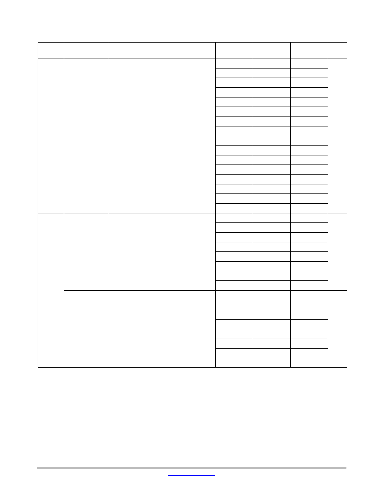
STATIC POWER CONSUMPTION (TA = +25°C)
Symbol
Parameter
Test Conditions
VCC (V)
(Note 18)
VL (V)
(Note 19)
Typ
Unit
(Note 20)
CPD_VL VL = Input port, CLoad = 0, f = 1 MHz,
VCC = Output Port EN = GND (outputs disabled)
0.9
4.5
0.01
pF
1.5
1.8
0.01
1.8
1.5
0.01
1.8
1.8
0.01
1.8
2.8
0.01
2.5
2.5
0.01
2.8
1.8
0.01
4.5
0.9
0.01
VCC = Input port, CLoad = 0, f = 1 MHz,
VL = Output Port EN = GND (outputs disabled)
0.9
4.5
0.01
pF
1.5
1.8
0.01
1.8
1.5
0.01
1.8
1.8
0.01
1.8
2.8
0.01
2.5
2.5
0.01
2.8
1.8
0.01
4.5
0.9
0.01
CPD_VCC VL = Input port, CLoad = 0, f = 1 MHz,
VCC = Output Port EN = GND (outputs disabled)
0.9
4.5
0.01
pF
1.5
1.8
0.01
1.8
1.5
0.01
1.8
1.8
0.01
1.8
2.8
0.01
2.5
2.5
0.01
2.8
1.8
0.01
4.5
0.9
0.01
VCC = Input port, CLoad = 0, f = 1 MHz,
VL = Output Port EN = GND (outputs disabled)
0.9
4.5
0.01
pF
1.5
1.8
0.01
1.8
1.5
0.01
1.8
1.8
0.01
1.8
2.8
0.01
2.5
2.5
0.01
2.8
1.8
0.01
4.5
0.9
0.01
18. VCC is the supply voltage associated with the I/O VCC port, and VCC ranges from +0.9 V to 4.5 V under normal operating conditions.
19. VL is the supply voltage associated with the I/O VL port, and VL ranges from +0.9 V to 4.5 V under normal operating conditions.
20. Typical values are at TA = +25°C
www.onsemi.com
9
Share Link: 