NJM3548 Просмотр технического описания (PDF) - Japan Radio Corporation
Номер в каталоге
Компоненты Описание
производитель
NJM3548 Datasheet PDF : 9 Pages
| |||
NJM3548
will once again turn the output off.
Due to a slight delay in the circuit, a high current transient will occur when the output is shorted to GND. This
current transient may reach 8 A during 5 µs. Consequently, switching at high frequencies with a shorted output
may destroy the circuit. If a short circuit condition is detected, stop switching the input and remove fault condition.
Thermal protection
The output of NJM3548 is equipped with a thermal shut-down function, that turns the outputs off at a chip (junction)
tenperature above typically 130°C.
Normal operation is resumed when the temperature has decreased about 20C.
Error functions
The Error indicating signal occurs on a separate pin. The complete error table is shown in figure 7.
The following conditions generate an error signal:
When the driver is activated and at least one of the following conditions has occurred:
• thermal overload
• short circuit to GND
• short circuit to VCC
• open circuit
An output current less than 8 mA might be detected as “open circuit”. Output currents larger than 8 mA and less
than 2 A will definitely not generate an error. The normal operational area is shown in figure 3.
Also when the driver is inactivated an Error indication can occur. That is if the output is shorted to VCC. In figure 4
short circuit to VCC Error state versus output voltage is shown.
When the Error-detection function is activated, the Error output is capable of sinking 8 mA, supporting direct
connection of an LED. The current has to be externally limited by a series resistor.
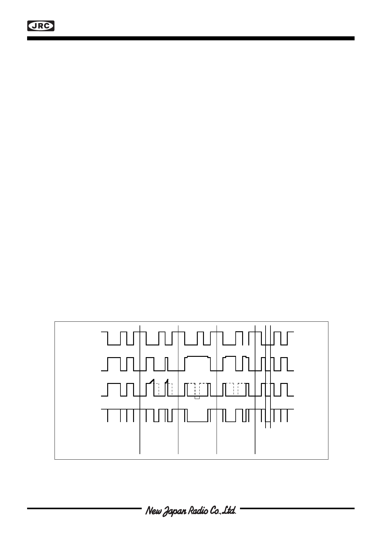
Signal diagrams
The signal diagram in figure 8 shows the input signal and the resulting output signals for each error mode. For
details, see error table, figure 7.
VIn = Input voltage. Active = LOW.
V = Output voltage.
Out
IOut = Output current from driver.
VErr = Error output voltage. Error = LOW.
VIN
VOUT
I OUT
VErr
Normal
operation
Overload or
short circuit
to GND
>130° <120°
Short circuit Open circuit Over
to VCC
temperature
Figure 8. Signal diagram
Share Link: 