NJM3548 Просмотр технического описания (PDF) - Japan Radio Corporation
Номер в каталоге
Компоненты Описание
производитель
NJM3548 Datasheet PDF : 9 Pages
| |||
s PIN CONFIGURATION
NJM3548
5
Output
4
Supply
3
GND
2
Input
1
Error
Figure 2. Pin Configuration
s PIN DESCRIPTION
TO-220
1
Symbol
Error
2
Input
3
GND
4
Supply
5
Output
Description
Error indicating pin. Sinks current to ground if the protection and/or detection circuitry is
activated.
Note: the current must be externally limited to 8 mA.
TTL compatible input. A HIGH input signal turns the output transistor off and a LOW
input turns it on. If the input is left open it will be detected as high level.
Ground supply.
Supply voltage. Nominally 5 V to 40 V.
Output pin. Current flows out from this pin through the load to GND. Nominal current is 8 mA
to 2 A.
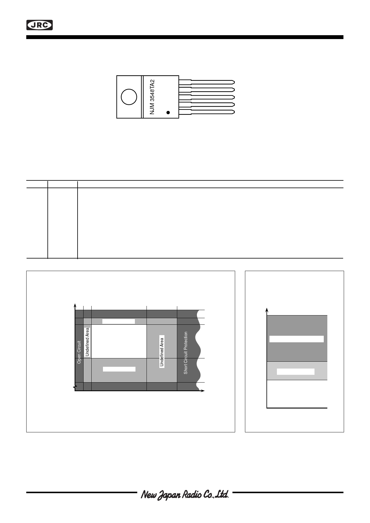
Output Voltage
VCC
VCC - 0.5 V
VCC - 1.3 V
NJM3548
Active Output
Short Circuit to VCC Error
Undefined Area
Normal
Operation
VCC - 3.0 V
Undefined Area
VCC - 4.5 V
Overload or Short Circuit to GND Error
IOMin
(min 2 mA, max 8 mA)
I OS
(min 2 A, max 4.5 A)
Output
Current
NJM3548
Output Voltage Inactive Output
100% VCC
Short Circuit to VCC Error
50% VCC
30% VCC
Undefined Area
Normal Operation
Figure 3. Error state vs. output voltage and output current, active output
(0V≤ VIN ≤ 0.8 V, 5 V < VCC < 40 V and -40°C <+TJ >+100°C)
Figure 4. Error state vs. output
voltage, inactive output (2.0 V ≤ VIN
≤ VCC, 5 V ≤ VCC ≤ 40 V and -40°C
<TJ <+100°C)
Share Link: 