HI5767/6IB Просмотр технического описания (PDF) - Intersil
Номер в каталоге
Компоненты Описание
производитель
HI5767/6IB Datasheet PDF : 15 Pages
| |||
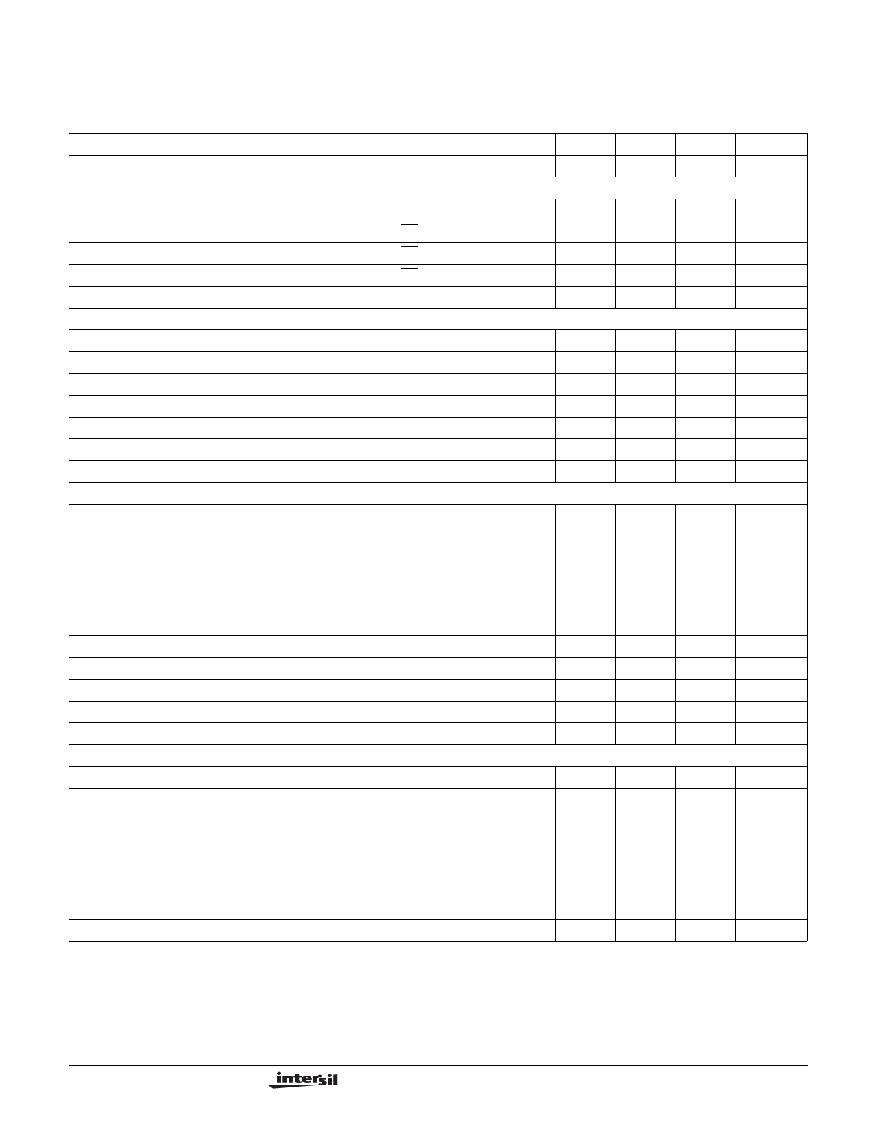
HI5767
Electrical Specifications
CAVL C=C10=pDFV; CTAC1==255o.0CV;,DDifVfeCrCen2t=ial3A.0nVa;loVgRIEnFpIuNt;=TVypRiEcaFlOVUaTl;ufeSs
= 40MSPS at 50% Duty Cycle;
are Test Results at 25oC,
Unless Otherwise Specified (Continued)
PARAMETER
TEST CONDITIONS
MIN
TYP
MAX
Maximum Output Current
-
-
0.2
DIGITAL INPUTS
Input Logic High Voltage, VIH
Input Logic Low Voltage, VIL
Input Logic High Current, IIH
Input Logic Low Current, IIL
Input Capacitance, CIN
DIGITAL OUTPUTS
CLK, DFS, OE
CLK, DFS, OE
CLK, DFS, OE, VIH = 5V
CLK, DFS, OE, VIL = 0V
2.0
-
-
-
-
0.8
-10.0
-
+10.0
-10.0
-
+10.0
-
7
-
Output Logic High Voltage, VOH
Output Logic Low Voltage, VOL
Output Three-State Leakage Current, IOZ
Output Logic High Voltage, VOH
Output Logic Low Voltage, VOL
Output Three-State Leakage Current, IOZ
Output Capacitance, COUT
TIMING CHARACTERISTICS
IOH = 100µA; DVCC2 = 5V
IOL = 100µA; DVCC2 = 5V
VO = 0/5V; DVCC2 = 5V
IOH = 100µA; DVCC2 = 3V
IOL = 100µA; DVCC2 = 3V
VO = 0/5V; DVCC2 = 3V
4.0
-
-
-
-
0.8
-10
±1
10
2.4
-
-
-
-
0.5
-10
±1
10
-
10
-
Aperture Delay, tAP
Aperture Jitter, tAJ
Data Output Hold, tH
Data Output Delay, tOD
Data Output Enable Time, tEN
Data Output Enable Time, tDIS
Data Latency, tLAT
Power-Up Initialization
For a Valid Sample (Note 2)
Data Invalid Time (Note 2)
-
5
-
-
5
-
-
5
-
-
6
-
-
5
-
-
5
-
-
-
7
-
-
20
Sample Clock Pulse Width (Low)
Sample Clock Pulse Width (High)
Sample Clock Duty Cycle Variation
POWER SUPPLY CHARACTERISTICS
fS = 40MSPS
fS = 40MSPS
fS = 40MSPS
11.3
12.5
-
11.3
12.5
-
-
±5
-
Analog Supply Voltage, AVCC
Digital Supply Voltage, DVCC1
Digital Output Supply Voltage, DVCC2
At 3.0V
At 5.0V
4.75
5.0
5.25
4.75
5.0
5.25
2.7
3.0
3.3
4.75
5.0
5.25
Supply Current, ICC
fIN = 1MHz and DFS = “0”
Power Dissipation
fIN = 1MHz and DFS = “0”
Offset Error Sensitivity, ∆VOS
AVCC or DVCC = 5V ±5%
Gain Error Sensitivity, ∆FSE
AVCC or DVCC = 5V ±5%
NOTES:
2. Parameter guaranteed by design or characterization and not production tested.
3. With the clock low and DC input.
-
62
-
-
310
-
-
± 0.7
-
-
± 0.1
-
UNITS
mA
V
V
µA
µA
pF
V
V
µA
V
V
µA
pF
ns
psRMS
ns
ns
ns
ns
Cycles
Cycles
ns
ns
%
V
V
V
V
mA
mW
LSB
LSB
7
Share Link: 