HI5710A Просмотр технического описания (PDF) - Intersil
Номер в каталоге
Компоненты Описание
производитель
HI5710A Datasheet PDF : 20 Pages
| |||
HI5710A
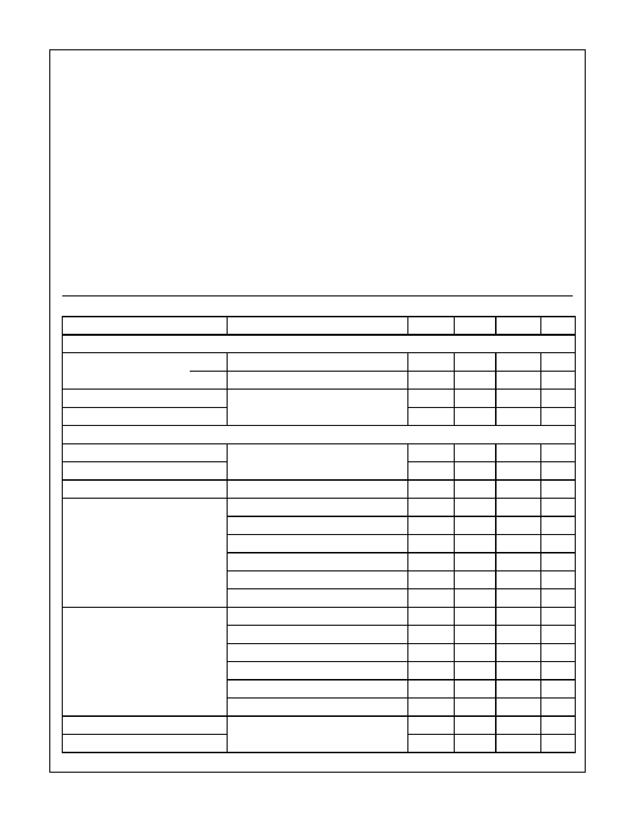
Absolute Maximum Ratings TA = 25oC
Supply Voltage, AVDD, DVDD. . . . . . . . . . . . . . . . . . . . . . . . . . . . 7V
Reference Voltage, VRT, VRB . . . . . . . . . VDD + 0.5V to VSS - 0.5V
Analog Input Voltage, VIN. . . . . . . . . . . . . VDD + 0.5V to VSS - 0.5V
Digital Input Voltage, VIH, VIL. . . . . . . . . . VDD + 0.5V to VSS - 0.5V
Digital Output Voltage, VOH, VOL . . . . . . . VDD + 0.5V to VSS - 0.5V
Thermal Information
Thermal Resistance (Typical, Note 1)
θJA (oC/W)
MQFP Package . . . . . . . . . . . . . . . . . . . . . . . . . . . .
111
Maximum Junction Temperature . . . . . . . . . . . . . . . . . . . . . . . 150oC
Maximum
Maximum
Storage Temperature Range,
Lead Temperature (Soldering
TSTG
10s) .
.
.
.
.
.
.
.
.
.-65oC
......
to
..
150oC
300oC
(Lead Tips Only)
Operating Conditions
Supply Voltage
AVDD, AVSS . . . . . . . . . . . . . . . . . . . . . . . . . . . . . . . . +5V ±0.25V
DVDD, DVSS . . . . . . . . . . . . . . . . . . . . . . . . . . +3.3V to 5V ±0.25V
|DGND-AGND| . . . . . . . . . . . . . . . . . . . . . . . . . . . .0mV to 100mV
Reference Input Voltage
VRB . . . . . . . . . . . . . . . . . . . . . . . . . . . . . . . . . . . . . . .1.8V to 2.8V
VRT . . . . . . . . . . . . . . . . . . . . . . . . . . . . . . . . . . . . . . .3.6V to 4.6V
Analog Input Range, VIN. . . . . . . .(VRT - VRB) (1.8VP-P to 2.8VP-P)
Clock Pulse Width
tPW1. . . . . . . . . . . . . . . . . . . . . . . . . . . . . . . . . . . . . . . .25ns (Min)
tPW0. . . . . . . . . . . . . . . . . . . . . . . . . . . . . . . . . . . . . . . .25ns (Min)
Temperature, TA . . . . . . . . . . . . . . . . . . . . . . . . . . . . .-20oC to 75oC
CAUTION: Stresses above those listed in “Absolute Maximum Ratings” may cause permanent damage to the device. This is a stress only rating and operation
of the device at these or any other conditions above those indicated in the operational sections of this specification is not implied.
NOTE:
1. θJA is measured with the component mounted on an evaluation PC board in free air.
Electrical Specifications fC = 20 MSPS, AVDD = +5V, DVDD = +3.3V, VRB = 2.0V, VRT = 4.0V, TA = 25oC (Note 2)
PARAMETER
TEST CONDITIONS
MIN
TYP
MAX UNIT
SYSTEM PERFORMANCE
Offset Voltage
Integral Non-Linearity, INL
Differential Non-Linearity, DNL
EOT
EOB
VIN = 2.0V to 4.0V
40
-120
-
-
90
-70
±1.3
±0.5
140
mV
-20
mV
±2.0
LSB
±1.0
LSB
DYNAMIC CHARACTERISTICS
Maximum Conversion Speed, fC
Minimum Conversion Speed, fC
Effective Number of Bits, ENOB
Signal to Noise and Distortion, SINAD
Spurious Free Dynamic Range, SFDR
Differential Gain Error, DG
Differential Phase Error, DP
fIN = 1kHz Ramp
fIN = 3MHz
fIN = 100kHz
fIN = 500kHz
fIN = 1MHz
fIN = 3MHz
fIN = 7MHz
fIN = 10MHz
fIN = 100kHz
fIN = 500kHz
fIN = 1MHz
fIN = 3MHz
fIN = 7MHz
fIN = 10MHz
NTSC 40 IRE Mod Ramp, fC = 14.3 MSPS
20
-
-
MSPS
-
-
0.5
MSPS
-
8.7
-
BIts
-
53
-
dB
-
52
-
dB
-
53
-
dB
-
54
-
dB
-
47
-
dB
-
45
-
dB
-
60
-
dB
-
59
-
dB
-
60
-
dB
-
65
-
dB
-
50
-
dB
-
49
-
dB
-
1.0
-
%
-
0.3
-
Degree
4-1533
Share Link: 