NCV8570 Просмотр технического описания (PDF) - ON Semiconductor
Номер в каталоге
Компоненты Описание
производитель
NCV8570 Datasheet PDF : 12 Pages
| |||
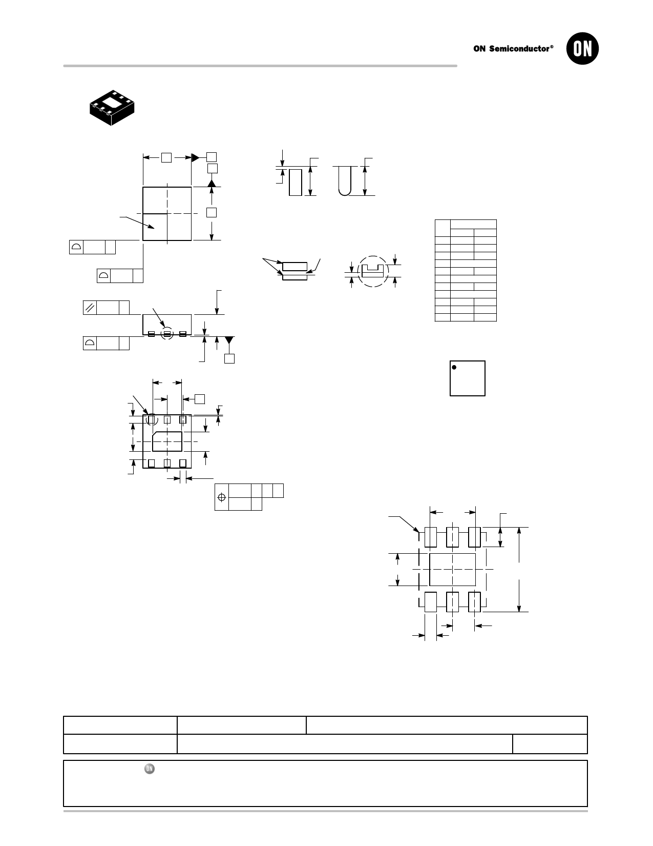
MECHANICAL CASE OUTLINE
PACKAGE DIMENSIONS
6
1
SCALE 4:1
DFN6, 2x2.2, 0.65P
CASE 506BA−01
ISSUE A
DATE 07 JUL 2008
D
A
B
L
L
L1
PIN ONE
REFERENCE
2X
0.10 C
ÉÉÉÉÉÉ
TOP VIEW
2X
0.10 C
E
DETAIL A
ALTERNATE TERMINAL
CONSTRUCTIONS
A3
EXPOSED Cu
MOLD CMPD
ÉÉÉÉÉÉ ÉÇÉÇ A
A1
0.10 C DETAIL B
DETAIL B
ALTERNATE
CONSTRUCTIONS
7X
0.08 C
SIDE VIEW
A1
C
SEATING
PLANE
D2
DETAIL A
6X L
1
e
3
6X L1
NOTES:
1. DIMENSIONING AND TOLERANCING PER
ASME Y14.5M, 1994.
2. CONTROLLING DIMENSION: MILLIMETERS.
3. DIMENSION b APPLIES TO PLATED TERMINAL
AND IS MEASURED BETWEEN 0.15 AND
0.20 mm FROM TERMINAL.
4. COPLANARITY APPLIES TO THE EXPOSED
PAD AS WELL AS THE TERMINALS.
MILLIMETERS
DIM MIN MAX
A 0.80 1.00
A1 0.00 0.05
b 0.20 0.30
D 2.00 BSC
D2 1.10 1.30
E 2.20 BSC
E2 0.70 0.90
e 0.65 BSC
K 0.20 −−−
L 0.25 0.35
L1 0.00 0.10
GENERIC
MARKING DIAGRAM*
1
XX MG
G
XX = Specific Device Code
M = Date Code
G = Pb−Free Device
E2
K
6
4
BOTTOM VIEW
6X b
0.10 C A B
0.05 C NOTE 3
*This information is generic. Please refer
to device data sheet for actual part
marking.
Pb−Free indicator, “G” or microdot “ G”,
may or may not be present.
PACKAGE
OUTLINE
SOLDERING FOOTPRINT*
1.36
6X
0.58
0.96
2.50
1
6X
0.35
0.65
PITCH
DIMENSIONS: MILLIMETERS
*For additional information on our Pb−Free strategy and soldering
details, please download the ON Semiconductor Soldering and
Mounting Techniques Reference Manual, SOLDERRM/D.
DOCUMENT NUMBER:
DESCRIPTION:
98AON23023D
Electronic versions are uncontrolled except when accessed directly from the Document Repository.
Printed versions are uncontrolled except when stamped “CONTROLLED COPY” in red.
6 PIN DFN, 2.0X2.2, 0.65P
PAGE 1 OF 1
ON Semiconductor and
are trademarks of Semiconductor Components Industries, LLC dba ON Semiconductor or its subsidiaries in the United States and/or other countries.
ON Semiconductor reserves the right to make changes without further notice to any products herein. ON Semiconductor makes no warranty, representation or guarantee regarding
the suitability of its products for any particular purpose, nor does ON Semiconductor assume any liability arising out of the application or use of any product or circuit, and specifically
disclaims any and all liability, including without limitation special, consequential or incidental damages. ON Semiconductor does not convey any license under its patent rights nor the
rights of others.
© Semiconductor Components Industries, LLC, 2019
www.onsemi.com
Share Link: 