NCV7361AD Просмотр технического описания (PDF) - ON Semiconductor
Номер в каталоге
Компоненты Описание
производитель
NCV7361AD Datasheet PDF : 27 Pages
| |||
NCV7361A
ELECTRICAL SPECIFICATIONS
All voltages are referenced to ground (GND). Positive
currents flow into the IC.
The maximum ratings (in accordance with IEC 134)
given in the table below are limiting values that do not lead
to a permanent damage of the device but exceeding any of
these limits may do so. Long term exposure to limiting
values may affect the reliability of the device. Correct
operating of the device can’t be guaranteed if any of these
limits are exceeded.
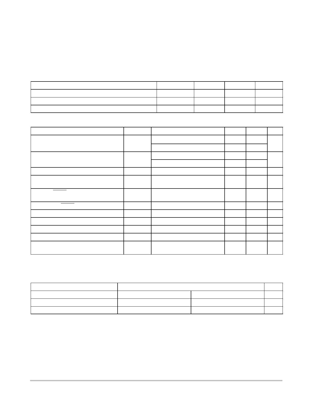
OPERATING CONDITIONS
Characteristic
Supply Voltage
Operating Ambient Temperature
Junction Temperature
Symbol
VSUP
TA
TJ
Min
Max
Unit
5.25
18
V
−40
+125
°C
−
+150
°C
MAXIMUM RATINGS
Rating
Symbol
Condition
Min
Max Unit
VSUP
BUS
Difference VSUP−VOUT
EN
VSUP
VBUS
VSUP−VOUT
VINEN
−
T v 500 ms
−
T v 500 ms
−
−
−1.0
30
V
−
40
−24
30
V
−
40
−0.3
40
V
−0.3
VSUP +
V
0.3
TxD, RxD, RESET
VIN
−
−0.3
VOUT +
V
0.3
EN, TxD, RxD, RESET
IIN
−
−25
25
mA
Short Circuit of Pin VSUP and VOUT
ESD Capability − All Pins
IINSH
ESDHB
−
Human Body Model, 100 pF via 1.5 kW
−500
−2.0
500
mA
2.0
kV
Junction Temperature
TJ
−
−
150
°C
Storage Temperature
Lead Temperature Soldering
Reflow: (SMD styles only)
TSTG
Tsld
−
60 second maximum above 183°C
−5°C/+0°C allowable conditions
−55
150
°C
−
240 peak °C
Stresses exceeding Maximum Ratings may damage the device. Maximum Ratings are stress ratings only. Functional operation above the
Recommended Operating Conditions is not implied. Extended exposure to stresses above the Recommended Operating Conditions may affect
device reliability.
THERMAL RATINGS
Parameter
Test Conditions Typical Value
SO−8 Package
Min−Pad Board (Note 1)
1.0 in Pad Board (Note 2)
Junction−to−Tab (psi−JL2, YJL2) (Note 3)
48
43
Junction−to−Ambient (RqJA, qJA)
183
120
1. 1 oz copper, 54 mm2 copper area, 0.062” thick FR4.
2. 1 oz copper, 714 mm2 copper area, 0.062” thick FR4.
3. psi−JL2 temperature was made at foot of lead #2.
Units
°C/W
°C/W
http://onsemi.com
3
Share Link: 