NCV4275A Просмотр технического описания (PDF) - ON Semiconductor
Номер в каталоге
Компоненты Описание
производитель
NCV4275A Datasheet PDF : 19 Pages
| |||
NCV4275A
APPLICATION INFORMATION
VI
II
CI1
CI2
I1
5Q
IQ
CQ
VQ
1000 μF
100 nF
NCV4275A
22 μF
Rext
5.0 k
ID
CD
D4
3
2 RO
IRO
VRO
47 nF
GND
Iq
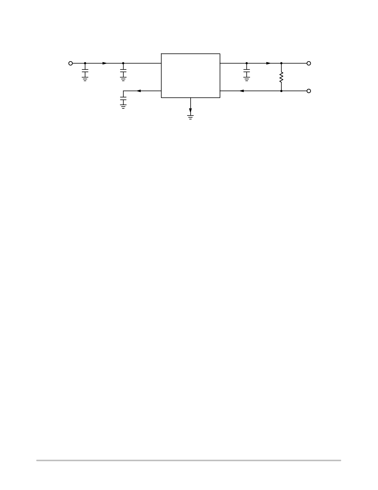
Figure 23. Test Circuit
Circuit Description
The NCV4275A is an integrated low dropout regulator that
provides 5.0 V or 3.3 V, 450 mA protected output and a signal
for power on reset. The regulation is provided by a PNP pass
transistor controlled by an error amplifier with a bandgap
reference, which gives it the lowest possible drop out voltage
and best possible temperature stability. The output current
capability is 450 mA, and the base drive quiescent current is
controlled to prevent over saturation when the input voltage
is low or when the output is overloaded. The regulator is
protected by both current limit and thermal shutdown.
Thermal shutdown occurs above 150°C to protect the IC
during overloads and extreme ambient temperatures. The
delay time for the reset output is adjustable by selection of the
timing capacitor. See Figure 23, Test Circuit, for circuit
element nomenclature illustration.
Regulator
The error amplifier compares the reference voltage to a
sample of the output voltage (VQ) and drives the base of a
PNP series pass transistor by a buffer. The reference is a
bandgap design to give it a temperature−stable output.
Saturation control of the PNP is a function of the load
current and input voltage. Over saturation of the output
power device is prevented, and quiescent current in the
ground pin is minimized.
Regulator Stability Considerations
The input capacitors (CI1 and CI2) are necessary to
stabilize the input impedance to avoid voltage line
influences. Using a resistor of approximately 1.0 W in
series with CI2 can stop potential oscillations caused by
stray inductance and capacitance.
The output capacitor helps determine three main
characteristics of a linear regulator: startup delay, load
transient response and loop stability. The capacitor value
and type should be based on cost, availability, size and
temperature constraints. A tantalum, aluminum or ceramic
capacitors can be used. The range of stability versus
capacitance, load current and capacitive ESR is illustrated
in Figures 2 to 5. Minimum ESR for CQ = 22 mF is native
ESR of ceramic capacitors. The aluminum electrolytic
capacitor is the least expensive solution, but, if the circuit
operates at low temperatures (−25°C to −40°C), both the
capacitance and ESR of the capacitor will vary considerably.
The capacitor manufacturer’s data sheet usually provides this
information.
The value for the output capacitor CQ shown in
Figure 23, Test Circuit, should work for most applications;
however, it is not necessarily the optimized solution.
Stability is guaranteed for CQ ≥ 22 mF and an ESR ≤ 4.5 W
(5.0 V Version), 3.5 W (3.3 V Version).
ESR characteristics were measured with ceramic
capacitors and additional resistors to emulate ESR. Murata
ceramic capacitors were used, GRM32ER71A226ME20
(22 mF, 10 V, X7R, 1210), GRM31MR71E105KA01 (1 mF,
25 V, X7R, 1206).
Reset Output
The reset output is used as the power on indicator to the
microcontroller. This signal indicates when the output
voltage is suitable for reliable operation of the controller.
It pulls low when the output is not considered to be ready.
RO is pulled up to VQ by an external resistor, typically
5.0 kW in value. The input and output conditions that
control the Reset Output and the relative timing are
illustrated in Figure 24, Reset Timing.
Output voltage regulation must be maintained for the delay
time before the reset output signals a valid condition. The
delay for the reset output is defined as the amount of time it
takes the timing capacitor on the delay pin to charge from a
residual voltage of 0.0 V to the upper timing threshold voltage
VDU. The charging current for this is ID,C and D pin voltage
in steady state is typically 3.2 V for 5.0 V regulator and
typically 2.4 V for 3.3 V regulator. By using typical IC
parameters with a 47 nF capacitor on the D pin, the following
time delay for 5.0 V regulator is derived:
tRD = CDVDU / ID,C
tRD = 47 nF (1.8 V) / 5.5 mA = 15.4 ms
Other time delays can be obtained by changing the
capacitor value.
http://onsemi.com
9
Share Link: 