NCP5500(2006) Просмотр технического описания (PDF) - ON Semiconductor
Номер в каталоге
Компоненты Описание
производитель
NCP5500 Datasheet PDF : 9 Pages
| |||
NCP5500, NCV5500, NCP5501, NCV5501
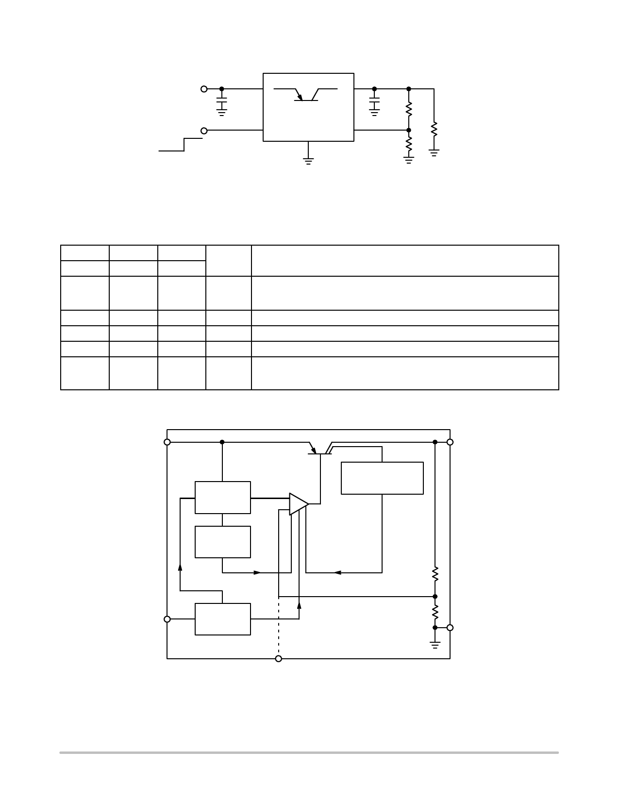
PIN FUNCTION DESCRIPTIONS
Pin No.
Symbol
Description
NCP5500 / NCV5500 − DPAK 5 Lead Center Lead Crop
1
EN
Output Enable; high level turns on the output.
2
IN
Input; battery/unregulated supply input voltage.
3, TAB
GND
Ground; Pin 3 connected internally to the Tab heat sink.
4
OUT
Output; bypass to ground.
5
NC / ADJ
No connection (Fixed output versions only).
Voltage−adjust input. Use an external voltage divider to set the output voltage over a
range of 1.25 V to 5.0 V. Adjustable version only.
NCP5501 / NCV5501 − DPAK 3 Lead
1
IN
Input; battery/unregulated supply input voltage.
2, TAB
GND
Ground; Pin 3 connected internally to the Tab heat sink.
3
OUT
Output; bypass to ground.
IN
Bandgap
Reference
Thermal
Shutdown
Error
Amplifier
−
+
Current Limit and
Saturation Sense
OUT
EN
EN and ADJ Pins
are applicable to
NCP5500 /
NCV5500 only.
Connection for Fixed Output
Connection for Enable
Connection for Adjustable Output
NC / ADJ
Figure 2. Block Diagram
GND
http://onsemi.com
2
Share Link: 